
Panasonic M12H switching power supply circuit diagram

Once saturation occurs, the voltage across the primary winding of T801 increases linearly, resulting in a DC voltage of 113V at pin 4 of IC801 while the transformer stores magnetic energy. As C806 continues to charge, the voltage at pin 2 of IC801 decreases, eventually causing the internal switch to exit saturation. When the switch is off, the current in the P1 and P2 windings of T801 decreases, causing the induced voltage polarities to reverse. This reduction in switch current leads to a rapid cycle of switching. After the switch turns off, the voltage at the S1 and S2 windings allows D801 to conduct, establishing a voltage of 16V across C810. Additionally, F1 and F3 windings allow D804 to conduct, releasing the stored magnetic energy from T801 to the 113V load. The discharging of the F2 and F3 windings through C806, R804, and D806 leads to a reverse charge at C806, which increases the voltage at pin 2 of IC801, facilitating the generation of flyback pulses through D805 and R805 that trigger the next oscillation cycle. The regulation of the circuit is managed automatically by the STR456A component. A protection circuit is included; if the 113V voltage rises excessively, R842 and R843 create a voltage drop that activates D837, leading to the conduction of SCR Q833, resulting in a short circuit of the 220V AC supply and blowing the fuse for safety.
This circuit design demonstrates a robust switching power supply mechanism, utilizing feedback loops for stabilization and regulation, while incorporating protective measures to prevent overvoltage conditions. The arrangement of components ensures efficient energy transfer and operational reliability across the specified Panasonic television models. As shown Panasonic M12H switching power supply circuit, the use of Panasonic movement M12H TV: Panasonic TC-230H, TC-2030DHN, TC-830D, TC-840D and the like. Oscillation Approxi mately 300V DC voltage on the C836, T801 all the way through the P1, P2 winding added IC801 (1) foot internal switching tube C pole, but added IC801 via R803 (2) foot internal switch B pole switch tube starts conducting, E pole current from IC801 (4) feet outflow. T801 of P1, P1 winding current increases, the induced voltage coupled to F2, F3 winding induced voltage polarity at this time F2, F3 winding is positive F2 F3 negative voltage through C806, R804 added IC801 (2 ), (4) feet, so that the switch current is further increased, a strong positive feedback switch rapidly saturated.
After saturation the switch, the voltage of the primary winding increases linearly T801, on the one hand in the IC801 (4) is formed pin 113V DC voltage, while T801 stored magnetic energy. With the C806 continue to be charged and the IC801 (2) pin voltage falling, and finally the internal switch out of saturation.
Once the switch out of saturation, T801 of P1, P2 winding current decreases, T801 each winding induced voltage polarity will flip, F2, F3 voltage winding and through C806, R804 to IC801 (2), (4 ) feet, so that switch current is further reduced, so the cycle to switch off quickly. After switching off, T801 S1, S2 voltage windings so D801 is turned on, the voltage on the establishment 16V C810; F1, F3 winding D804 also allows conduction, T801 stored magnetic energy is released by the D804 to 113V load, while the C806 through R804, D806, T801 of F2, F3 winding discharge, 300V voltage by R803 to C806 reverse charging, so (2) IC801 pin voltage rise, the line flyback pulses also through D805, R805 to IC801 (2) feet, IC801 advance turned on to start another cycle of oscillation.
Regulator circuit Regulator circuit is done automatically by STR456A inside. Protection circuit If 113V voltage increases, the R842, R843 partial pressure after D837 conduction, SCR Q833 conduction, 220V AC is short-circuited, the fuse burned.
Related Circuits

A CMOS logic gate is utilized in this circuit. When an object approaches the antenna, the change in oscillator output is detected by components 1)1 and 1)2, which is then amplified by U1C. This amplification drives Q1, activating alarm...
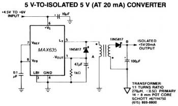
A negative output voltage DC to DC converter generates a -5V output at pin A. To achieve -5V at point A, the primary of the transformer must fly back to a diode drop more negative than -5V. If the...
1988 Honda Civic Tail Light Wiring Diagram. The 1988 Honda Civic tail light wiring diagram provides a detailed representation of the electrical connections and components associated with the tail light system of the vehicle. This schematic typically includes information on...
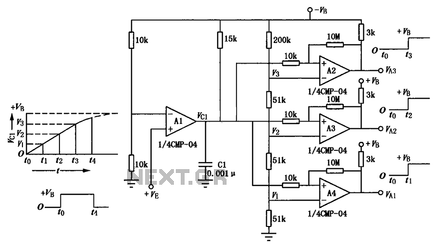
A multi-stage delay circuit is presented in this schematic. The operational amplifiers are configured as comparators. Operational amplifier A1 operates when the voltage at the inverting input exceeds + VE. As the voltage at the inverting input of operational...

The circuit depicted features a double oscillator utilizing a monostable multivibrator CC4098 and a quad 2-input NAND gate CC4011, among other components. This circuit allows for adjustable frequency and duty cycle. It is primarily designed as a keying oscillator,...
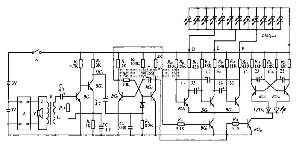
The BGl and BG2 form a directly coupled amplifier, while BG and BG4 consist of a monostable trigger circuit. Without receiving a prior trigger signal, BG3 enters a saturated conduction state. During this steady state, the collector of BG4...