
Basic circuit diagram connection of signal and power INA166

The INA166 is a precision instrumentation amplifier designed for high common-mode rejection and low noise operation. The circuit configuration requires careful attention to component placement and values to optimize performance. The use of a 0.1 µF tantalum capacitor at the power supply terminal is essential for stabilizing the power input and filtering out high-frequency noise, which can adversely affect the amplifier's performance. The PCB layout should minimize the distance between the capacitor and the chip to reduce inductive effects, which can introduce voltage drops and noise.
For the sense output voltage detection, the reference terminal must be connected with low resistance to maintain the integrity of the common-mode rejection ratio. This is critical in applications where the amplifier is subjected to varying common-mode voltages, as a higher common-mode rejection results in improved accuracy and signal fidelity. The specification indicates that introducing a 5-ohm series resistor can significantly reduce the common-mode rejection ratio, which must be avoided to ensure optimal performance.
The internal gain structure of the INA166 is designed to provide a high overall gain of 2000, with the first two stages contributing significantly to this gain. The input stages A1 and A2 have a gain of 200, while the output stage A3 amplifies the signal with a gain of 10. The addition of a gain-setting resistor RG between pins 3 and 12 allows for further customization of the amplifier's gain, making it adaptable to various applications. The gain formula, G = 2000 + 60000/RG, illustrates how the choice of RG directly influences the overall gain, allowing for precise adjustments based on the specific requirements of the circuit.
Overall, careful consideration of component selection, placement, and circuit design is essential for maximizing the performance of the INA166 in precision measurement applications. Proper adherence to these guidelines will ensure that the amplifier operates effectively, providing accurate and reliable signal amplification. As shown for the basic connection circuit INA166 signals and power. Chip power supply terminal to use 0.1 F tantalum capacitor filter, PCB layout should be as close to the chip tantalum capacitor power pin placement. Sense output voltage detection terminal connection, the connection must be reference terminal Ref low resistance connections to ensure a high common mode rejection ratio, if 5 series resistor will result in the common-mode rejection ratio decreased. Internal fixed gain of 2000, wherein the input stage A1, A2 gain 200, the gain of the output stage 10 A3.
Between 3 feet and 12 feet to increase a gain setting resistor, RG can change the amplifier gain, the gain G 2000 + 60000/RG.
Related Circuits

This design circuit is for audio graphic equalizers, which are commonly found in commercial products, yet circuits for them are rarely published. The circuit features a simple design that requires an operational amplifier (op-amp) to amplify the input signal....
The Phase-Locked Loop (PLL) will synchronize with an input signal, providing both triangle and square wave outputs. A quad operational amplifier can be utilized in this circuit, making it suitable for audio and low-frequency radio applications. The Phase-Locked Loop (PLL)...
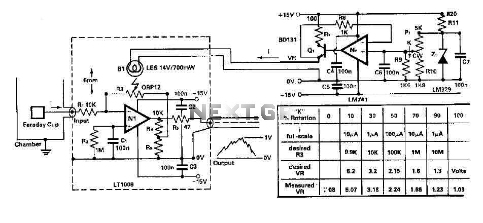
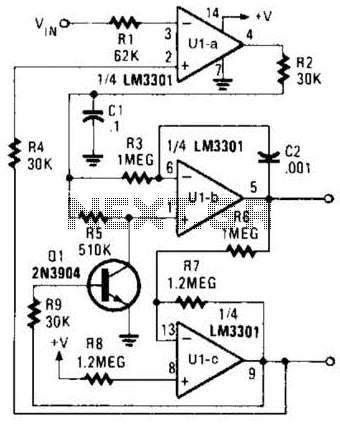
To amplify small current signals as an electron collector inside a vacuum chamber, it is advantageous for reasons related to noise and bandwidth to have a "head-amplifier" connected to the chamber. Operational amplifier 1 is a precision device featuring...

A BA1404 integrated circuit (IC) is utilized to generate a complete FM multiplex (MPX) signal. The chip incorporates all necessary circuitry. Components CI, R3, R4, and C4 are responsible for providing pre-emphasis. The transmitter operates on a single AA...
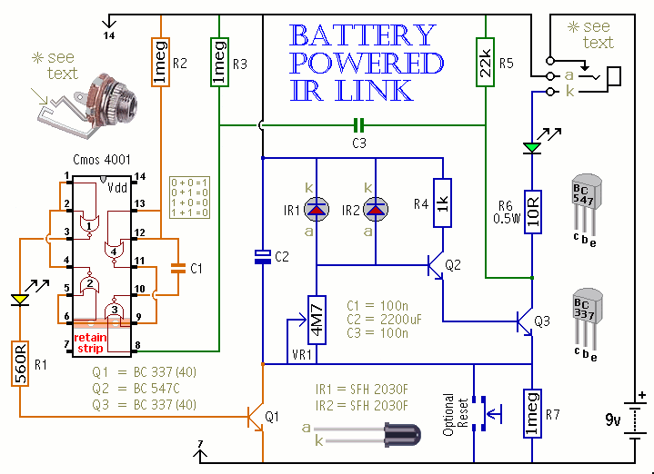
This is a battery-powered infrared (IR) link that can be utilized in multiple rooms. The standby current is exceptionally low, resulting in excellent battery life. The circuit is designed to shut down when faced with extraneous IR radiation, effectively...
The ICM7226 is a fully integrated Universal Counter and LED Display driver. It combines a high-frequency oscillator, a decade timebase counter, an 8-decade data counter and latches, a 7-segment decoder, digit multiplexer, and segment and digit drivers, which can...