
1.3W RF Amplifier

The RF amplifier circuit is critical for applications requiring signal enhancement, such as in communication systems. The primary function of this circuit is to increase the power level of the RF signal while preserving its integrity. The 2SC1970 transistor is chosen for its favorable characteristics, including high gain and frequency response, making it suitable for RF applications.
The circuit typically consists of several key components: the NPN transistor, biasing resistors, coupling capacitors, and possibly an output transformer for impedance matching. The biasing resistors ensure that the transistor operates in the active region, allowing for linear amplification. Coupling capacitors are used to block DC components while allowing AC signals to pass, ensuring that the RF signal is amplified without distortion.
The input RF signal is fed into the base of the transistor, where it is amplified by the transistor's gain factor. The amplified output is taken from the collector, where it can be further processed or transmitted. The design may also include feedback mechanisms to stabilize the gain and improve linearity, as well as bypass capacitors to filter out noise.
For optimal performance, careful consideration must be given to the layout of the circuit. Minimizing parasitic capacitance and inductance is essential, particularly at high frequencies, to maintain signal integrity. Additionally, the power supply must be adequately decoupled to prevent fluctuations that could affect the amplifier's performance.
In summary, this RF amplifier circuit schematic provides a robust solution for amplifying RF signals, leveraging the capabilities of the 2SC1970 transistor while allowing for flexibility in component selection to meet specific application requirements.This diagram is a schematic diagram of RF amplifier circuit. The circuit will amplify the RF signal about times, 100mW input power to 1.3W output power. It use a general NPN RF transistor 2SC1970. You may apply other transistors, for exa.. 🔗 External reference
Related Circuits

The LM317 integrated circuit (IC) is commonly recognized as a voltage regulator; however, it can also function as an audio amplifier. This low-power amplifier circuit designed with the LM317 provides a maximum output of approximately 1 watt. The LM317...
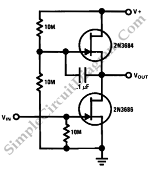
This is a simple high-gain JFET audio amplifier circuit. This circuit requires very low power but provides a high-gain amplification function. It is also referred to as JFET. The JFET (Junction Field Effect Transistor) audio amplifier circuit is designed to...
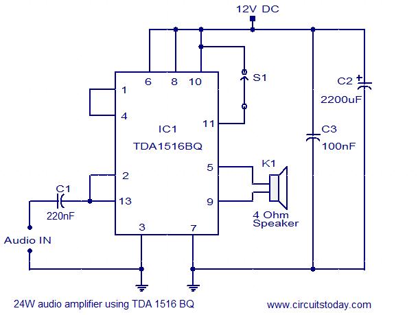
The circuit diagram illustrates a simple 24W mono amplifier utilizing the TDA1516 integrated circuit. The TDA1516 is a Class B power amplifier packaged in a 13-pin SIL configuration. This integrated circuit includes several beneficial features, including short circuit protection,...
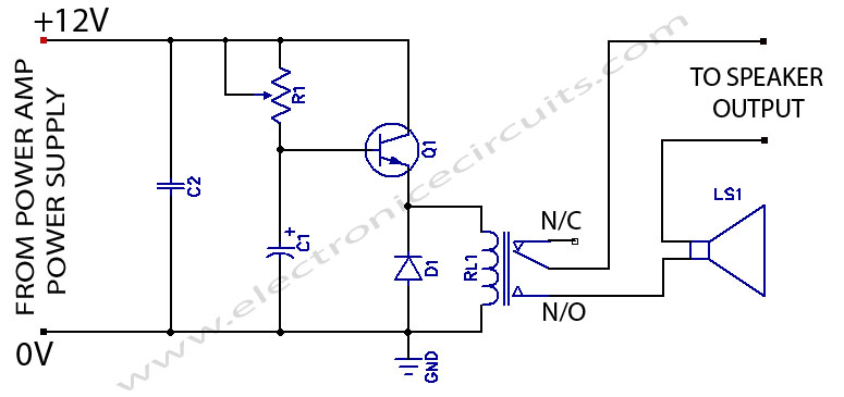
When powering on a power amplifier, a loud thump sound occurs due to a sudden heavy discharge current through the speaker. This current has the potential to damage the speaker, particularly in the case of a direct-coupled amplifier. The phenomenon...
Stationary - MOPLL & Silicon Tuner TUA6020 2 Band TV Tuner Mixer-Oscillator-PLL with balanced IF-Amplifier. The TUA6020 device integrates a digitally programmable Phase Locked Loop (PLL) with a mixer-oscillator block that includes two balanced mixers and oscillators suitable for...

This circuit is very basic to build and puts out great power for your car or home. Keep all leads as short as possible. This circuit is designed to deliver substantial power output suitable for automotive or residential applications. The...