
100W FM Linear Amplifier

The described power amplifier utilizes the MRF317 bipolar transistor, which is well-regarded for its performance in RF applications, particularly in FM broadcasting. The Class C biasing configuration employed in this circuit is optimal for high-efficiency applications, as it allows the transistor to conduct for less than half of the input signal cycle, thereby maximizing power output while minimizing heat generation.
The impedance matching networks for both the input and output stages are crucial for ensuring maximum power transfer and minimizing signal reflection. These networks have been designed using Mimp.EXE software, which aids in the precise calculation of component values to achieve the desired frequency response. The inclusion of a 9-element low pass filter at the output stage is particularly noteworthy, as it serves to attenuate unwanted harmonics and spurious signals, ensuring compliance with regulatory standards by providing at least 60 dB of rejection from the carrier frequency. The RF simulation performed with RFSIM99 further validates the design, allowing for adjustments based on simulated performance metrics.
The amplifier's gain of 10 dB indicates a substantial increase in signal strength, making it suitable for various FM transmission applications. The efficiency rating of 60 to 65% suggests that a significant portion of the input power is converted into useful output power, which is a critical factor in the design of power amplifiers to reduce operational costs and thermal management issues.
The input Voltage Standing Wave Ratio (VSWR) of approximately 1.4 indicates good impedance matching, which minimizes reflections and maximizes power delivery from the source to the amplifier. This characteristic is essential for maintaining the integrity of the transmitted signal across the entire FM band, ensuring that the amplifier can operate effectively without distortion or loss of quality.
Overall, this power amplifier design is well-suited for FM broadcasting applications, providing a balance of efficiency, gain, and signal integrity.This Power amplifier is equiped with a bipolar transistor,the famous MRF317. As lots of FM amplifier application ,the power transistor is in a C class bias. All the impedance networks (Input & Output) have been determined by using the software: Mimp.EXE. A 9 elements low pass filter ensures that we meet at least a 60 dB rejection from the carrier.(RF Simulation with RFSIM99). The FM amplifier has a 10 dB gain with a 60 to 65% efficiency. The Input VSWR is around 1.4 and there's no problem to reach the max power in all the FM band.. 🔗 External reference
Related Circuits

A Class-A audio amplifier is known for its high power consumption; however, its simplicity is appealing when ample power is available. This circuit features a Darlington transistor designed for use with a 5-volt power supply. It is important to...
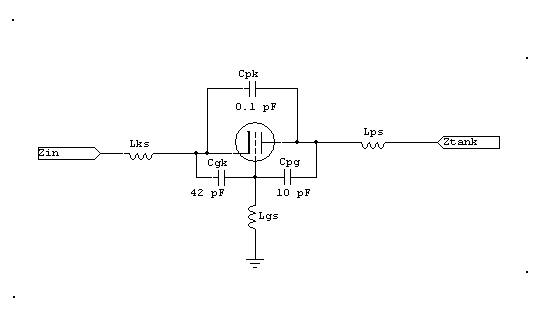
Grid-driven tetrodes such as the 6146, 807, or 4CX250 exhibit high power gain. High-gain systems require minimal feedback to remain stable, which necessitates neutralization. Additionally, these systems often need a grid loading resistor to stabilize or reduce gain. The...
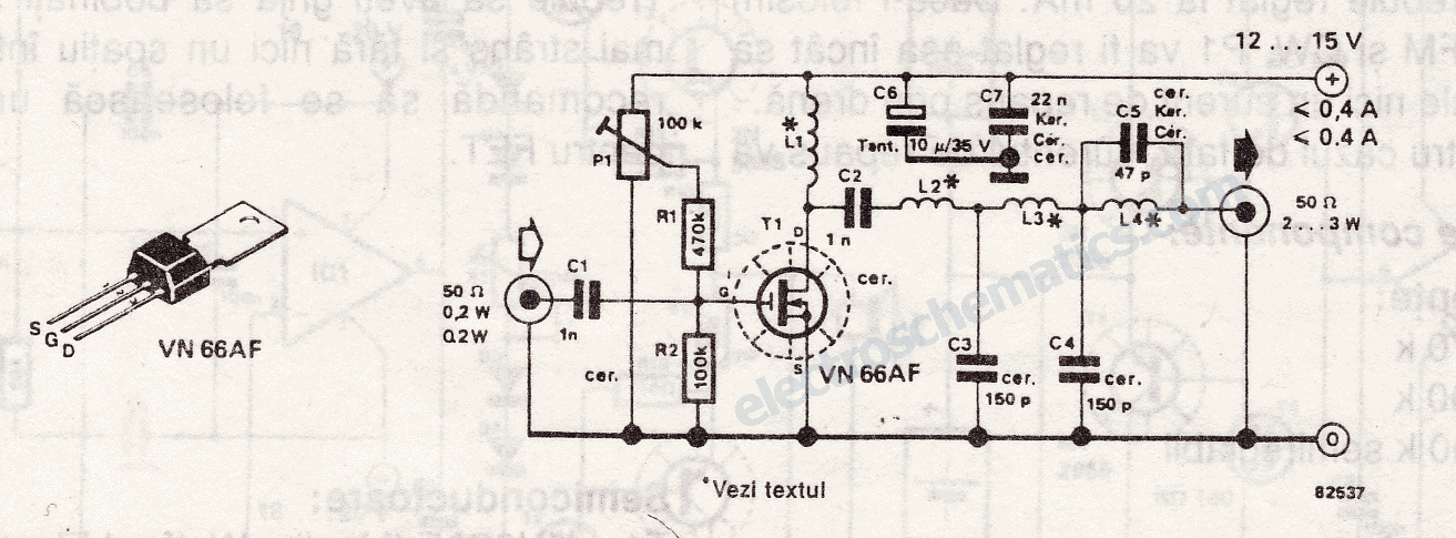
The 10-meter 27MHz continuous wave (CW) radio amplifier is equipped with the VN66AF transistor produced by Siliconix, which offers several advantages: it is inexpensive, provides excellent dielectric insulation, and has high gain. The VN66AF is utilized as an RF...
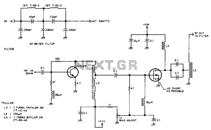
The circuit illustrated is designed to generate up to 5 watts of RF output in the 40-meter (7 MHz) amateur band. The coils depicted are wound on toroidal cores from Armdon Associates Inc., with part numbers provided in the...
This is a circuit schematic diagram for a power amplifier utilizing the IC TLE2141C. The TLE2141C is a low-noise, high-voltage, high-slew-rate operational amplifier. It offers a frequency response from 30 Hz to 20 kHz with a variation of 1...

This circuit utilizes the ZTX450 and ZTX550 transistors configured in a push-pull output stage. The following measurements were recorded at maximum volume: Input: 0.4 mV rms, Output: 1.8 V rms, Voltage gain: 4500, Maximum output before distortion: 2.25 V...