
1024KHz temperature compensation crystal oscillator circuit diagram

The 1024 kHz temperature-compensated crystal oscillator circuit is designed to provide a stable frequency output that remains consistent despite variations in temperature. Central to this design is a crystal oscillator, which utilizes a quartz crystal to maintain frequency accuracy. The oscillator generates a low-level output signal, which necessitates the inclusion of a transistor buffer stage for signal amplification.
In this configuration, the transistor VT1 acts as a buffer amplifier. The base of VT1 is biased by resistor R2, which sets the operating point and ensures that the transistor remains in the active region for linear amplification. Resistor R3, connected to the collector of VT1, serves as the load resistor, determining the gain of the amplifier and affecting the output signal level. The emitter resistor R4 introduces negative feedback into the circuit, which stabilizes the DC operating point of VT1 and enhances linearity by reducing distortion.
Additionally, the use of a Zener diode in the circuit provides voltage regulation, ensuring that fluctuations in supply voltage do not adversely affect the oscillator's performance. This arrangement allows the circuit to maintain a consistent output frequency of 1024 kHz across a range of temperatures, making it suitable for various applications where precise timing is essential. Overall, this circuit design exemplifies effective use of feedback and amplification techniques to achieve reliable frequency generation.This circuit SJT is 1024kHz temperature compensation crystal oscillator. Circuit theoryis asshown. Because output signal level of the circuit is low, the buffer of follow-up transistor VTl is amplified. VTl base bias resistor R2, the load resistor R3, the emitter resistor R4 are the negative feedback resistors for stablizing VTl DC operating point.
Zener.. 🔗 External reference
Related Circuits
This document presents plans for a simple ground plane antenna that is effective in the FM band (88-108 MHz). It is constructed from a small plastic disk. The 6 x 6 loop antenna, designed by Graham Maynard, is highlighted...

The saving lamp circuit features two main types: glass cover and exposed. The glass cover variants include three series: spherical, cylindrical, and processing types. The first two series consist of four variations: transparent, carved, engraved, and white. These lamps...
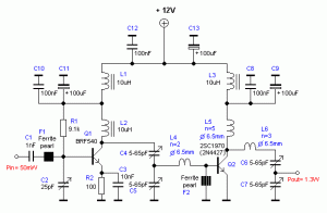
The RF power amplifier circuit described here utilizes the transistors 2SC1970 and 2N4427. This FM RF amplifier operates within the frequency range of 88-108 MHz, delivering an output power of approximately 1.3W from an input driver of 30-50mW. The...

The circuit utilizes an LM122 timer, as illustrated in Figure 1, to manage various timing operations, including starting, resetting, and halting the process midway through. The operation of the circuit is governed by switching mechanisms. Switch S1 initiates the...
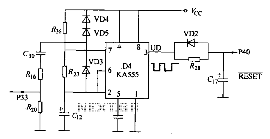
Anti-jamming circuit (watchdog circuit): KA555 interference when analog baseband circuit is shown in Figure 18-14. The KA555 is a hybrid analog/digital integrated circuit. The input signal is connected to specific pins, while the power supply is 5V and the...
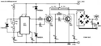
This inverter circuit is designed to power electric razors, stroboscopes, flash tubes, and small fluorescent lamps using a 12-volt car battery. Unlike typical feedback oscillator inverters, this design features a separate oscillator from the output stage, allowing for easy...