
12vdc to 220vac inverter with sine wave output

The described circuit consists of two channels that operate in a Class D configuration, commonly used for efficient amplification of low-frequency signals, particularly in the Very Low Frequency (VLF) range. Each channel is composed of a combination of diodes (DA3, DA5 for the first channel and DA4, DA7 for the second channel) and transistors (VT1, VT2 for the first channel and VT3, VT4 for the second channel).
The diodes serve to rectify and shape the input signals, ensuring that only the desired portions of the waveform are amplified. The transistors act as the primary amplifying elements, switching on and off rapidly to create a pulse-width modulated (PWM) signal that corresponds to the input sine wave. This method of amplification is highly efficient, as it minimizes power loss in the form of heat.
The outputs of the two channels produce sine waves that are 180 degrees out of phase with each other. This antiphase output is critical for applications that require differential signaling or for driving a load that benefits from such a configuration, such as a push-pull driver for a speaker or other transducer.
The overall design requires careful consideration of component selection, including the characteristics of the diodes and transistors, to ensure optimal performance in the VLF range. Additionally, attention must be paid to the layout of the circuit to minimize interference and ensure stable operation. Proper filtering may also be necessary at the output to smooth the PWM signal into a clean sine wave, depending on the specific application requirements.In DA3, DA5, VT1, VT2 assembled the first channel of the VLF class D. The second channel, respectively, collected on DA4, DA7, VT3, VT4. At the output of the first and second channels are formed antiphase sine wave VLF 🔗 External reference
Related Circuits
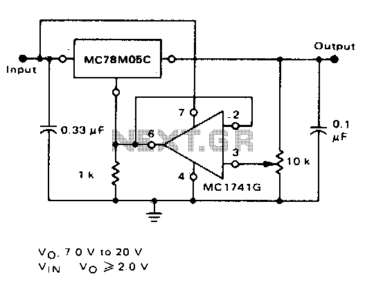
The inclusion of an operational amplifier facilitates the adjustment to higher or intermediate voltage levels while maintaining regulatory characteristics. The minimum voltage achievable with this configuration is 2 volts above the regulator voltage. The circuit employs an operational amplifier (op-amp)...
The circuit output voltage can be continuously adjusted from zero to its maximum value. The baseline is established by a constant current sourced from the auxiliary power supply circuit. The reference current of 500 microamperes can be fine-tuned to...
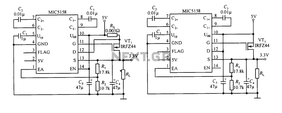
The circuit consists of peripheral components for the MIC5158, a linear regulator that converts a 5V input into a 3.3V output with a maximum current of 10A. When the input voltage (Ui) is 5V, an N-channel MOSFET, specifically the...
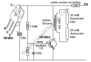
A 40-watt fluorescent tube lamp or two 20-watt tubes in series will be driven by this circuit. The transformer is wound on a ferrite rod with a diameter of 10 mm and a length of 8 cm. The circuit described...
The circuit serves as a foundational design, requiring experimentation for specific applications. In popular microwave bands, local oscillators (LOs) are typically generated using overtone crystal oscillators followed by multipliers. A table presents the standard LO frequencies for narrowband segments,...

The circuit presented in this article illustrates a straightforward method for constructing a compact inverter that is easy to assemble and offers the functionality of a pure sine wave inverter. The design can be easily modified to achieve higher...