
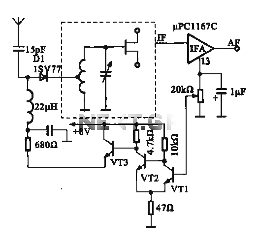
1W FM Transmitter Circuit

The 1-watt FM transmitter circuit operates by utilizing a series of transistors to amplify and stabilize the radio frequency (RF) signal. The first transistor serves as the oscillator, generating the RF signal at the desired frequency. This is critical as the frequency stability directly impacts the clarity and range of the transmitted signal. The buffer stage, which follows the oscillator, is essential for isolating the oscillator from the load, thereby preventing any frequency drift that may occur during adjustments.
The resonance stage (T3) is designed to enhance the output power and efficiency of the transmitter. It utilizes a variable capacitor to fine-tune the frequency response, ensuring that the transmitter operates at optimal performance. The final amplification stage, which is the heart of the transmitter, is where the output power is significantly increased to the desired level, with a focus on maintaining linearity and minimizing distortion.
The choice of transistors is crucial; the 2N4427 is favored for its efficiency and performance in the RF range, while alternatives like the BD139 or 2N2219 can be used with certain limitations. It is important to ensure that the selected transistor can handle the operating frequency and power levels without overheating, necessitating the use of heatsinks where required.
Adjustment of the trimmers throughout the circuit is a vital step in achieving maximum output power and ensuring proper function. The use of resistors at the RF output during testing helps in safely measuring and adjusting the output power before finalizing the antenna connection.
Finally, the power supply specifications, including the 12V DC requirement and the current consumption, provide essential information for the design and implementation of the circuit, ensuring that it operates reliably and efficiently within its intended application. Proper thermal management and component selection will enhance the longevity and performance of the transmitter, making it suitable for various broadcasting needs.A very good 1 watt fm transmitter circuit, very easy to build circuit. It has 4 transistors, one is a very stable oscillator, followed by a buffer stage to prevent frequency variation when you adjust the transmitter. Next is a resonance stage and the final stage built with a minimum 1W transistor which must have a heatsink.
You must use a LM7805 s tabilizer for the oscillator diodes and one LM7809 for powering up the T1 oscillator stage. This will give you a very stable transmitter frequency. First build the oscillator stage and the buffer, power it up and trim the 10k linear potentiometer untill you can here a blank signal on your receiver. If you put a small piece of wire on the T2 emitter you can see that the cover range of the 2 stage transmitter is about 3 meter.
After you are sure that your oscillator+buffer stage are working properly, remove the power supply and continue building the T3 resonance stage. Connect the power supply and if you adjust the trimmer (variable capacitor) from T3 collector you can see how the fm transmitter power can be varied.
This stage is very important for proper functionality of the entire 1 watt fm transmitter. You must adjust the trimmer for maximum power. The final stage of the 1W fm transmitter is built with 2N4427 (recommended) or the transistors from the list. If you can`t find any, use a BD139 transistor but only for frequencies lower than 90 MHz. The output power will be lower but you get the idea. If you decide to use 2N2219 transistor for the final stage of the transmitter you must know that the output rf power will be 0.
4W. Adjust the last 2 trimmers for maximum output power in the antenna. Initially use 2 x 100 © 0. 5W resistors in parallel at the RF output. Then connect this rf probe to the output and adjust all the 3 trimmers starting from T3 to output. You must adjust it to obtain the maximum multimeter indication. Then power it off, connect the antenna and make the final adjustments for maximum broadcasting coverage distance. Use a 12Vdc power supply to power up this fm broadcast circuit. T4 will have a current consumption of around 150 mA at full power output adjustments. The total current consumption of the entire 1 watt transmitter will be around 500 mA. 🔗 External reference
Related Circuits
This circuit illustrates an FM modulator with a strong and weak signal switching mechanism. The circuit diagram 3-14 (a) depicts mechanical switches, including a worker selector switch that allows for signal strength selection. Figure 3-14 (b) demonstrates the implementation...

How to create a hydrogen generator using a 555 timer circuit with Pulse Width Modulation (PWM). This PWM circuit can generate hydrogen on demand. The hydrogen generator circuit utilizing a 555 timer operates by controlling the duty cycle of the...
This humidity detector circuit diagram is straightforward and utilizes a limited number of components. It can be employed to activate electronic devices when the detector identifies a specific humidity level. The sensor is made from two copper pieces positioned...

This circuit diagram for a logic tutor kit was created using MS Word graphics. While modern software is commonly utilized, there may be instances where traditional methods are necessary. Employ a sharp pencil and a ruler to ensure precision;...

The PGA202 offset voltage correction circuit is designed to correct both input and output offset voltages. There are four different gain settings for the PGA202, which result in slight variations in input offset voltage. A 50k potentiometer is used...

This circuit utilizes the exceptionally low input current of 0.1 pA from the CA3420 BiMOS operational amplifier. It employs a single 10-MΩ resistor. The circuit operates within a range of ±50 pA, achieving a maximum full-scale sensitivity of ±1.5...