
2800w high power audio amplifier

The mono high power amplifier circuit is designed to deliver a maximum output of 1400 W, making it suitable for high-performance audio applications. To achieve stereo sound, the circuit must be duplicated, resulting in a total output capability of 2800 W. This necessitates careful consideration of the power supply, PCB layout, and thermal management to accommodate the increased power demands.
The schematic provided illustrates the basic configuration of the amplifier, which includes gain stages utilizing two JRC4558 operational amplifiers. These op-amps are known for their low noise and high fidelity, which is essential for maintaining audio quality in high power applications. The configuration typically involves using the op-amps in a differential amplifier setup to enhance the signal before it is sent to the output stage.
The amplifier circuit also incorporates various transistors that serve as buffers and drivers. These transistors are critical for managing the current flow and ensuring that the amplifier can drive low-impedance loads without distortion. The choice of transistors will affect the overall performance, including factors such as bandwidth, linearity, and thermal stability.
The booster section of the amplifier, which has not yet been implemented in the current design, is vital for achieving the desired output power levels. This section would typically include additional transistors configured in a push-pull arrangement to drive the output stage effectively. The layout should ensure minimal signal degradation and adequate heat dissipation, as high power levels can generate significant heat.
In summary, the presented high power amplifier circuit is a robust design that, while currently incomplete, lays the foundation for a high-performance audio system. Future enhancements, particularly in the booster stage, will be necessary to realize the full potential of the amplifier in stereo applications.Mono high power amplifier is actually a powerful 1400 W, but if this hihgh power amplifier circuit is doubled and you want to create stereo, high power amplifier the necessary components and pcb requires two-fold. So if the stereo high power amplifier 2 X 1400W. Schematic Circuit diagram is still less by looking at the circuit that was so below, t he finished circuit has been added with a gains using JRC4558 IC by the two and the picture ic where it can be seen below. For circuit buffers, drivers, and booster use multiple transistors and other components (can be seen listed component).
And high power amplifier project that is so below is just part of the buffer and driver while the booster has not been made. For additional transistors in the booster or high power amplifier end scheme can be found Booster output power amplifier.
🔗 External reference
Related Circuits
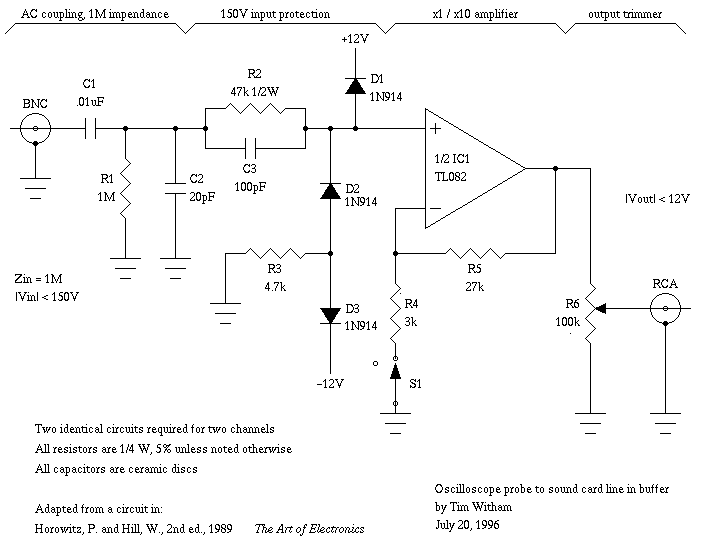
For capacitor C3, a 100pF capacitor is placed across resistor R2. The circuit functions similarly to previous configurations, although no explanation is provided. The purpose of this component may be self-evident to experienced users, but it may not be...
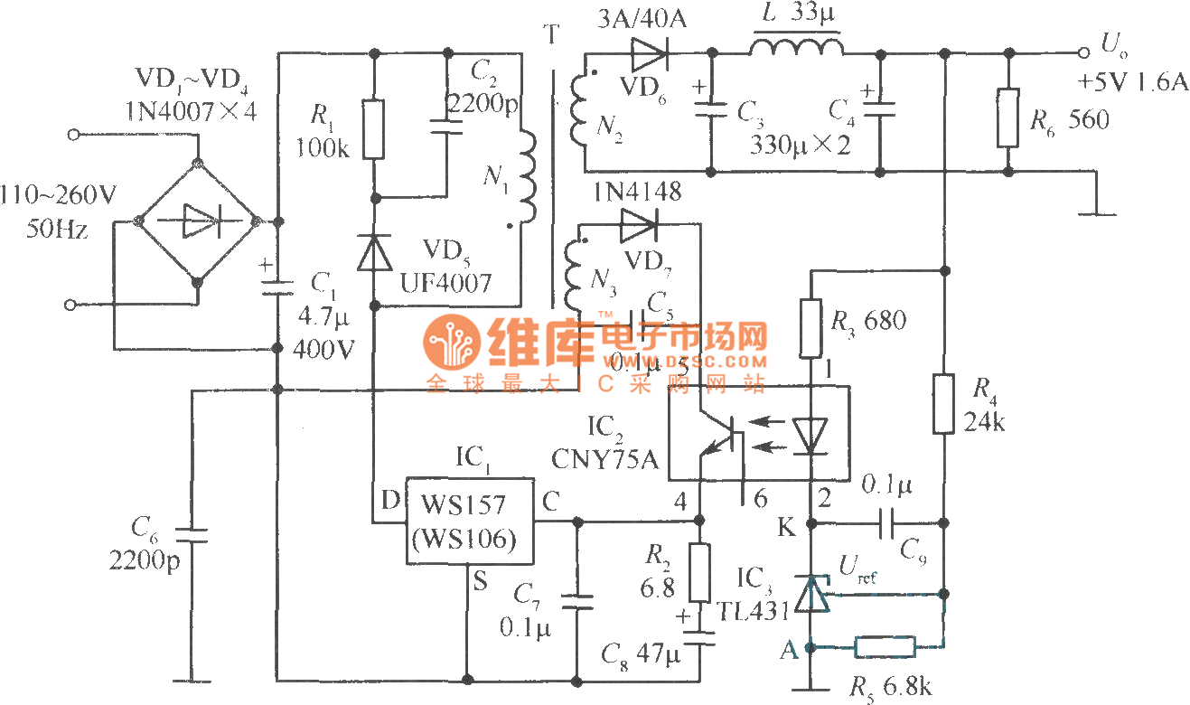
The +5V, 1.6A precision switching power supply circuit is depicted in the figure. This circuit utilizes a photoelectric coupler (CNY75A) and an adjustable precision parallel regulator (TIA31). R3 serves as the current limiting resistor, while R4 and R5 function...
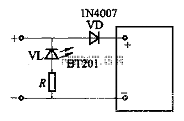
The adjustment potentiometer RP allows for modification of the over-voltage limit setting. In the event of reversed polarity in the DC power supply, there is a risk of damaging equipment components. To mitigate this risk, a reverse polarity protection...
The LV2282VA is an FM Transmitter integrated circuit (IC). The multiplex (MPX) block generates a stereo modulated composite signal from left (L) and right (R) audio inputs. The radio frequency voltage-controlled oscillator (RF VCO) incorporates an FM modulation function....
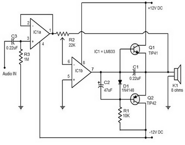
The 15W Class B audio amplifier circuit presented here is a straightforward Class B audio amplifier utilizing the TL082 operational amplifier, along with TIP41 and TIP42 transistors. The LM833 is a dual amplifier known for its high scanning speed...
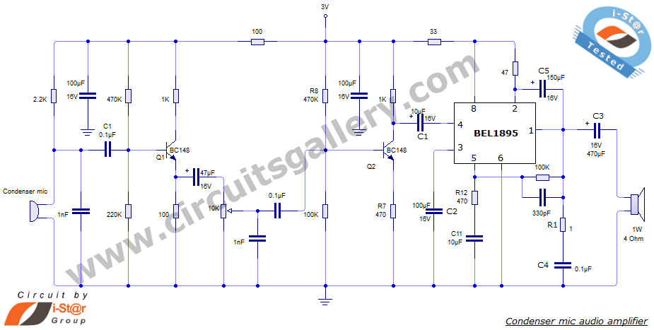
This document presents an audio amplifier circuit suitable for use in walkie-talkies, low-power transmitters, and packet radio receivers. The circuit utilizes a condenser microphone audio amplifier that delivers high-quality audio output of 0.5 watts at 3 volts. The design...