
2n2907 For7-Segment Digital Clock Circuit

The Clock Controller V1.1 circuit is designed to manage timing and control functions in electronic applications. The primary component, the 2N2907 transistor, is a general-purpose PNP transistor capable of handling moderate currents, making it suitable for switching applications. The configuration of pins P3.0 to P3.3 indicates that these pins can be utilized as control signals to activate or deactivate the transistor, allowing it to sink current effectively.
In this setup, when a high signal is applied to any of the pins P3.0 to P3.3, the base of the PNP transistor becomes forward-biased, allowing current to flow from the collector to the emitter. This action enables the transistor to act as a switch, controlling the load connected to its collector. The load can be any device that requires a controlled power supply, such as an LED, motor, or relay.
The circuit may also include additional components such as resistors to limit the base current and protect the transistor from excessive current flow. A pull-up resistor may be employed to ensure that the transistor remains off when the control pins are not actively driven high. Furthermore, bypass capacitors could be integrated to filter any noise from the power supply, ensuring stable operation of the Clock Controller.
Overall, the Clock Controller V1.1 circuit provides a versatile solution for timing and control in various electronic systems, leveraging the capabilities of the 2N2907 transistor to manage current flow based on the signals from the microcontroller or other digital logic devices.Circuit above shows a circuit diagram of the Clock Controller V1.1. P3.0-P3.3 also drives a base pin of 4-PNP transistor, 2n2907 with sink current .. 🔗 External reference
Related Circuits
This power supply utilizes a single 7812 IC voltage regulator along with multiple external pass transistors, enabling it to deliver output load currents of up to 30 amps. The circuit design incorporates a 7812 linear voltage regulator, which is...
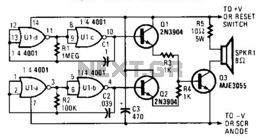
An external horn-type speaker is optimal for this circuit. However, such devices demand significant power, so this sounder should only be employed in alarm circuits utilizing at least a 6-A SCR as the sounder driver. The circuit incorporates a...
The semiconductor thermistor is an embedded thermal protection element that is sensitive to temperature, with a temperature error of 5 degrees. It offers reliability, a small size (diameter 3.5 mm), and ease of installation, making it suitable for embedding...
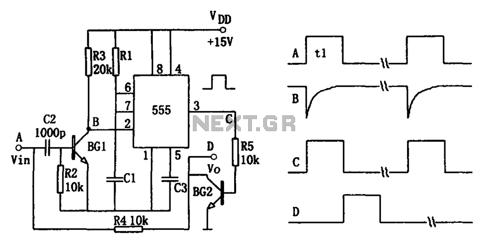
The pulse-width detection circuit is illustrated in the figure and consists of a differential circuit (R2, C2), an amplifier (BG1), a single stabilizing circuit (555, R1, C1), and various other components. The pulse signal Vin (depicted as waveform A)...
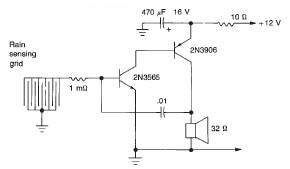
This rain detector electronic circuit project is a simple alarm circuit that activates an audio warning when liquid is detected on the sense pad. The circuit diagram is based on two transistors. When the sense pad conducts, transistors Tr1...
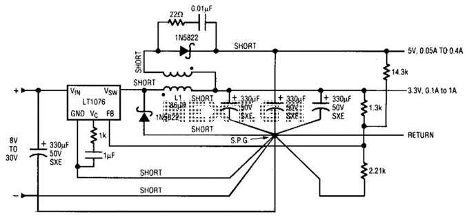
Input voltages can range from 8 V to 30 V. The load range for the 5 V output is from 0.05 A to 5 A, while the load range for the 3.3 V output is from 0.1 A to...