
3-6V Xenon Strobe Light

This circuit design effectively demonstrates the functionality of the 555 timer in PWM applications while employing high-voltage components safely and efficiently. The careful arrangement of components, including the MOSFET, transformers, capacitors, and diodes, ensures the desired operation of the flash circuit while highlighting the importance of safety measures when dealing with high voltages. Proper understanding of the circuit operation and component behavior is essential for anyone considering replicating or modifying this design.This circuit used to come as a kit from a surplus supplier, but probably isn`t available anymore. It shows a few novel concepts such as using a 555 as a pulse width modulator (PWM), and series/parallel camera flash transformers. WARNING: This circuit is contains voltages and currents which can KILL if you are not careful. Charged capacitors will S URPRISE YOU! They can hold a lethal charge for hours! If you don`t know much about working with high voltages or if you aren`t crazy (like me) then DO NOT attempt to construct this circuit. I CANNOT BE RESPONSIBLE if you electrocute yourself to death! That said, let`s have some fun! The 555 is set up as a pulse width modulator (the off (low) time being set by the trimmer). The output at pin 3 is connected to the gate of the P-channel MOSFET (IRF9Z20) through the 100R resistor to prevent parasitic oscillation of the transistor.
A low signal at pin 3 causes the MOSFET to turn on, thus the potentiometer controls the output power, and somewhat the flash frequency, by varying the duty cycle of the 555 and in turn the MOSFET. The drain of the MOSFET transistor is connected to the primaries of T1-T4 - the camera flash transformers.
These primary windings are connected in series, and being originally intended to operate at 3V, this allows an input voltage of 12V. In this particular series/parallel configuration, the secondaries of T1-T4 are connected in parallel, supplying approximately their rated 330V, but at 4 times the current since there are 4 of them.
This is rectified by the 1N4005 diode and passed along to the 150u storage capacitor. Also, the 6n9 and 12n capacitors are charged. Once the 6n8 cap reaches the strike voltage of the neon lamp, which is approximately 60V, it is dumped into the gate of the SCR, turning it on. This in turn dumps the 12n capacitor into the primary of the trigger transformer, T5. This is stepped up to around 3kV and applied to the glass envelope of the Xenon flash tube. Through the capacitance of the glass, this voltage is passed through to the Xenon gas inside, ionizing it and creating a conductive channel for the discharge of the 150u capacitor.
The 2u8 inductor widens out this discharge, creating a slightly longer flash. This circuit demonstrates how the 555 can be used as a PWM. You can see in the schematic how the two diodes are connected between pins 2/6 and pin 7. The 3k potentiometer connected as shown sets the on time of the 555 (Off time of the MOSFET), but if another potentiometer is connected between pin 7 and the other diode, the off time can also be adjusted. The way the circuit is drawn in the schematic above, the off time is basically fixed. The MOSFET is on during the off time of the 555 because when it`s off, pin 3 is connected to ground, so another way of saying it is that it goes low.
Then when the 555 goes high again, or back to positive rail voltage, the internal capacitance of the MOSFET is shorted out which shuts it off. Everyone seems to assume people know this. It`s different from regular bipolar junction transistors because in a bipolar, if you disconnect base current, it conveniently just shuts off as long as there is no current flowing.
Now, because of the way a FET works, there is a sort of capacitor formed between the gate and channel. Just removing the voltage source does not shut the FET down. This is because of the capacitor, the electric field is still present and it just keeps going. So if your gate input doesn`t discharge this capacitor, you will need to use what is called a or pull up (P-channel) or pull down (N-channel) resistor beteween the gate and source.
In this case though, we don`t need it because the 555 automatically pulls itself up and down for us. Gotta love that 555! T1-T4 are 4 identical Kodak Ektralite camera flash transformers. The brand name isn`t important, just that they`re itentical. They have ferrite cores like most camera flash transformer 🔗 External reference
Related Circuits
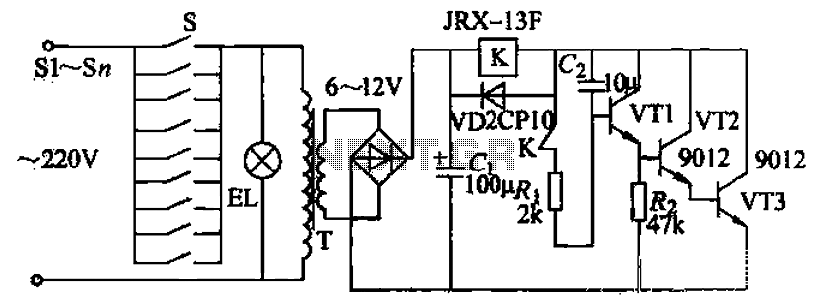
Pressing the button switch Sl-Sn activates the circuit, turning on the transformer T. The low-voltage alternating current from the secondary winding is directed to a bridge rectifier and a filter capacitor Ci, which produces a DC voltage. This voltage...

Figure 2-78 illustrates the SH-841 as the central component in a holiday lights controller. It utilizes SCRs VS1 to VS4 to drive light strings H1 to H4, causing them to flash. The operating voltage is sourced from AC through...
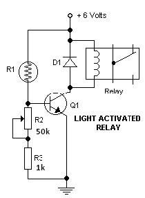
This light-dark switch activated relay circuit schematic represents one of the simplest electronic circuits designed to activate other electronic devices based on light or darkness. It requires a single electronic relay and a few common components that are not...

The example programs and Arduino sketches provided are free software. The provided example programs and Arduino sketches serve as a valuable resource for developers and hobbyists working with Arduino microcontrollers. These software tools are designed to facilitate learning and experimentation...
The following circuit illustrates a Sun Up Alarm Light Alarm Circuit Diagram. This circuit is based on the 555 Integrated Circuit (IC). Features include simplicity and cost-effectiveness. The Sun Up Alarm Light Alarm Circuit employs the 555 timer IC in...
This circuit is designed to drive a total of 42 LEDs, assuming a forward voltage of approximately 2.2V per LED and a forward current of around 21mA for adequate brightness. If the specifications of the LEDs differ significantly, modifications...