
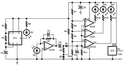
3 Band graphic equalizer circuit

The circuit operates by utilizing the LF351 operational amplifier, which is known for its low noise and high bandwidth characteristics, making it ideal for audio applications. The inverting amplifier configuration ensures that the output signal is inverted relative to the input, which is a typical requirement in equalizer circuits to maintain signal integrity while allowing for gain adjustments.
The filter network consists of passive components, including resistors and capacitors, designed to create bandpass filters centered around the specified frequencies. Each bandpass filter is tuned to either enhance or attenuate the audio signal within its designated frequency range. The use of potentiometers for R1, R2, and R3 allows for user interaction, enabling the fine-tuning of the audio output according to personal preferences or specific acoustic environments.
In practical applications, this three-band graphic equalizer can be integrated into audio processing equipment, such as mixers, amplifiers, or home audio systems, providing users with the ability to customize sound output effectively. The circuit design promotes simplicity and efficiency, making it accessible for both amateur and professional audio engineers. The overall design emphasizes reliability and performance, ensuring that the audio quality is preserved while allowing for significant control over the frequency response of the audio signal.Here is the circuit diagram of a simple 3 band graphic equalizer circuit using a single IC and few components. The IC used here is LF 351 which is a wide bandwidth single JFET operational amplifier. The high input impedance of the IC makes this circuit compatible with most of the audio signal sources.
The opamp is wired as an inverting amplifier. The input signal is fed to the inverting input of the opamp via the filter network. The filter network can produce a +/- 20 dB enhancement or cut on the three frequency bands 50Hz, 1KHz and 10KHz. POTs R1, R2 and R3 can be used for adjusting the gain of the different bands. 🔗 External reference
Related Circuits

A wideband RF detector is being designed, utilizing a series of resonant LC tanks spaced between 5 to 10 MHz apart, with an exception of 1 MHz spacing from 9 MHz onwards. The design of a wideband RF detector incorporating...
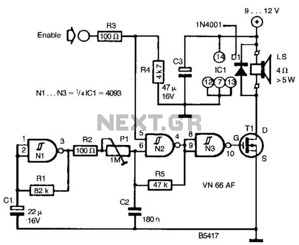
A CD4093 chip and several components form a siren oscillator that drives power MOSFET Tl. A speaker is directly powered by this device. The siren is activated by a logic high signal applied to the ENABLE input. The circuit comprises...
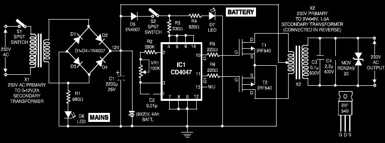
This circuit diagram of a UPS is designed for use with cordless telephones that cannot operate during a power failure. Since the UPS is intended solely for telephones, its output power is limited to 1.5W. This UPS circuit is...
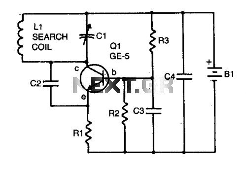
The locator utilizes a transistor radio as the detector. By tuning the radio to a weak station, the capacitor C1 can be adjusted so that the locator's oscillator beats against the received signal. When the search head passes over...
This circuit was designed to assist in parking a car near a garage wall while reversing. LED D7 lights up when the distance to the wall is approximately 20 cm. When the distance reduces to about 10 cm, both...
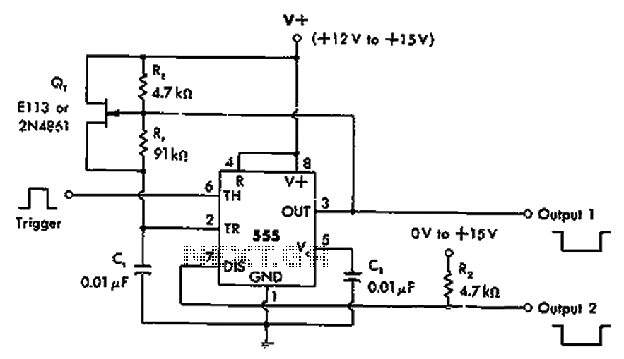
The timer 555 is activated by a positive trigger pulse, which results in negative output pulses. In scenarios where the duty cycle exceeds 99%, heavy loads can be disconnected from pin 7 without impacting timing accuracy, although loads exceeding...