
45Mhz If Amplifier With Crystal Filter Circuit

The 40673 dual-gate MOSFET is designed for RF amplification applications, particularly suitable for use in high-frequency circuits such as those involving crystal filters. In this configuration, the MOSFET is matched to a crystal filter that operates at a frequency of 45 MHz, which is a common frequency for various communication systems. The impedance of the filter, approximately 2 kΩ, is significant as it influences the matching network design to ensure optimal power transfer and minimal signal reflection.
The gain control feature, facilitated by a variable +4 V source that can be adjusted down to -4 V, allows for dynamic adjustment of the amplifier's performance. This capability is critical in applications where signal conditions may vary, enabling the user to maintain consistent output levels. The dual-gate configuration of the MOSFET provides enhanced control over the gain, allowing for improved linearity and reduced distortion, which is particularly beneficial in RF applications.
For implementation, it is essential to design a matching network that accommodates the 2 kΩ impedance of the crystal filter while ensuring that the 40673 MOSFET operates within its specified parameters. This may involve the use of inductors and capacitors to create a suitable impedance transformation. Additionally, attention should be given to power supply decoupling and layout considerations to minimize parasitic capacitances and inductances, which can adversely affect performance at high frequencies.
Overall, the integration of the 40673 dual-gate MOSFET with a crystal filter at 45 MHz presents a robust solution for RF amplification, with the added benefit of gain control to adapt to varying signal conditions. A 40673 dual-gate MOSFET is matched to a crystal filter at 45 MHz. The filter impedance is around 2kQ. The + 4-V source can be made variable for gain control ( about +4 to -4V.)
Related Circuits
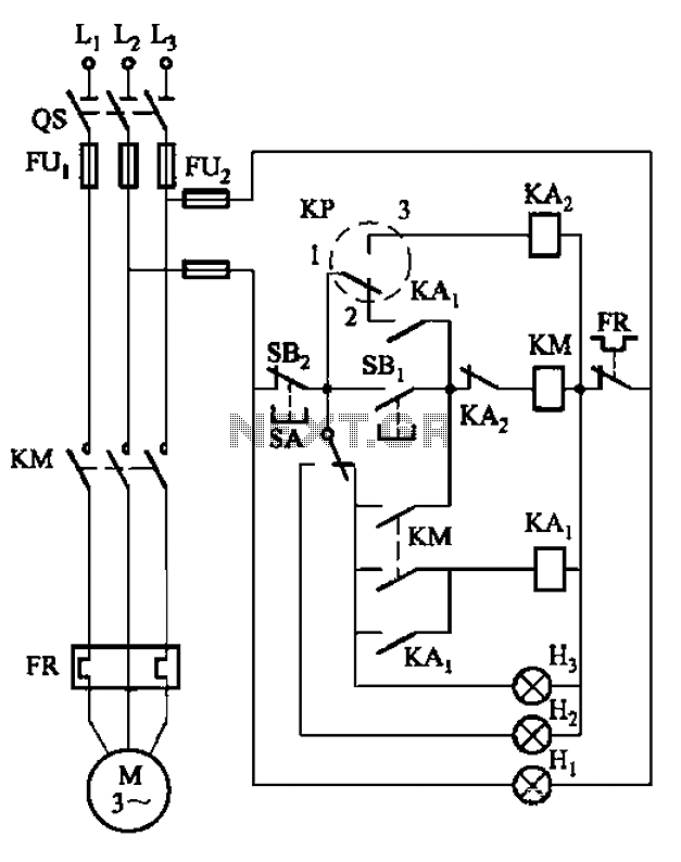
An air compressor is commonly utilized in electrical equipment factories and is typically controlled by electrical contacts. The circuit diagram is depicted in Figure 5-1. The circuit allows for both automatic and manual operation. In the diagram, KP represents...
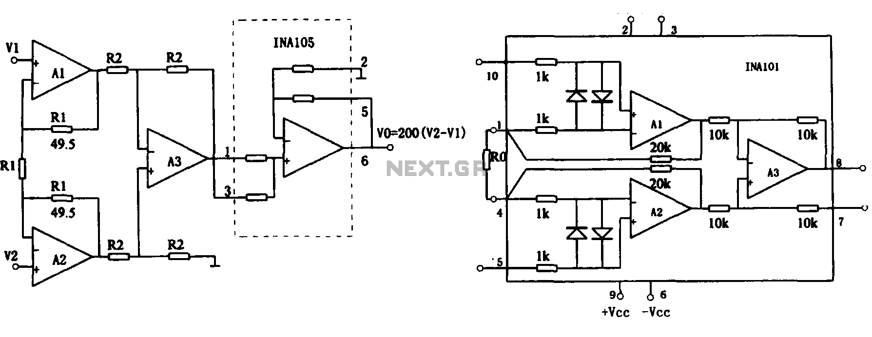
This document describes the extended common mode input voltage range of an instrument amplifier circuit. The circuit consists of three precision instrument amplifiers, A1, A2, and A3, which can be INA101 or INA102 models. The figure illustrates that A1,...

This simple wind charger circuit project is designed using the LTC1042 monolithic CMOS window comparator, manufactured by Linear Technology. The wind charger circuit utilizes wind power to generate the energy necessary for charging Ni-Cd or lead-acid batteries. When the...
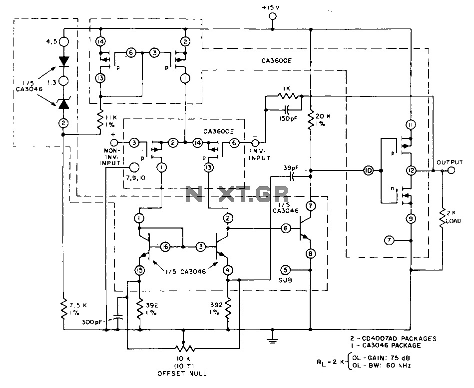
This unity-gain follower amplifier features a CMOS p-channel input, an NPN second-gain stage, and a CMOS inverter output. The integrated circuit components consist of two CA3600E CMOS transistor pairs and a CA3046 NPN transistor array. A zener-regulated leg provides...
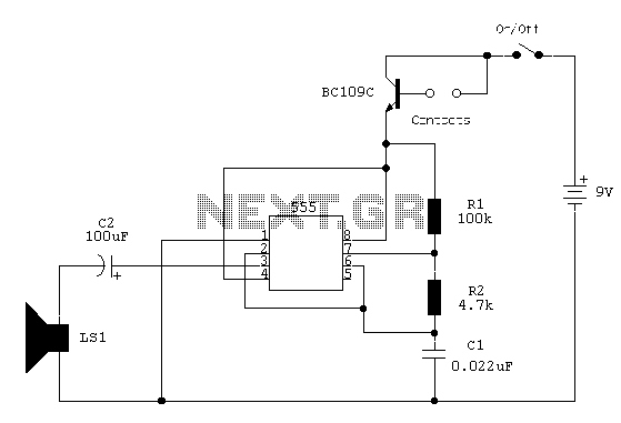
The circuit utilizes a 555 timer configured as an astable oscillator, powered by the emitter current of a BC109C transistor. In dry conditions, the transistor remains off due to the absence of bias current. However, when the probes become...
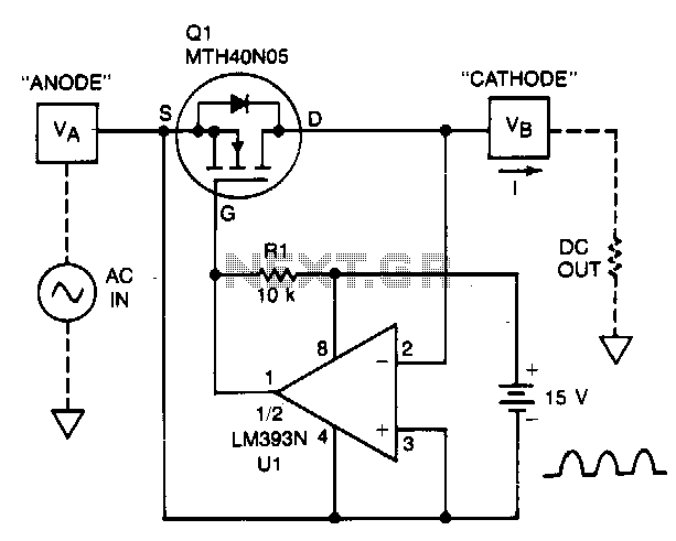
A TMOS power FET, Q1, and an LM393 comparator provide a high-efficiency rectifier circuit. When voltage V1 exceeds V2, the output of U1 becomes high, and Q1 conducts. Conversely, when V2 exceeds V1, the comparator output becomes low, and...