
Extended common mode range of the instrumentation amplifier (INA101) circuit
")
The described instrument amplifier circuit is designed to handle a wide common mode input voltage range, making it suitable for various applications requiring high precision. The use of INA101 or INA102 as the primary amplifiers (A1, A2, A3) ensures that the circuit maintains high accuracy and low noise characteristics. These amplifiers are known for their low offset voltage and drift, which are critical in sensitive measurement applications.
The configuration of the INA105 as a unity gain amplifier in output follower mode is significant for maintaining the integrity of the signal while providing additional voltage gain. The parallel arrangement of the four resistors within the INA105 circuit contributes to achieving a voltage amplification factor of 2, while ensuring that the input impedance remains high, thus minimizing the loading effect on the source.
The total amplification of 200 times indicates that the circuit is capable of significantly boosting weak signals, making it ideal for applications in instrumentation where the detection of small changes in voltage is necessary. The high input impedance (in the megohm range) further enhances the circuit's performance by allowing it to interface effectively with high-impedance sensors without affecting their operation.
The internal structure of the INA101, as shown in figure (b), provides insights into the design and functionality of the amplifier, revealing the arrangement of transistors, resistors, and other components that contribute to its operational characteristics. This detailed understanding of the internal architecture can aid in troubleshooting and optimizing the circuit for specific applications.Shown for the extended common mode input voltage range of the instrument amplifier circuit. The circuit A1, A2 and A3 can be precision instrument amplifier INA101 or INA102 constitution. The figure shows, A1, A2 and A3 voltage magnification l00 times, then using precision amplifier unity gain amplifier INA105, connection to the amplifier inverting input, output follower mode, four resistors were about to internal circuit in parallel, thus obtained INA105 amplifier voltage amplification factor of 2 and a high input impedance (megohm). Total voltage of the circuit 200-fold magnification. Figure (b) is the internal structure of the INA101.
Related Circuits
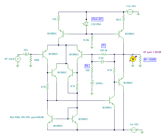
This circuit was submitted by Graham Maynard from Newtownabbey, Northern Ireland. It has an exceptionally fast high-frequency response, as demonstrated by applying a 100kHz square wave to the input. All graphs were produced using Tina Pro. The circuit in question...
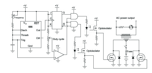
A common topology for DC-AC power converter circuits employs a pair of transistors to switch DC current through the center-tapped winding of a step-up transformer. Examine the check plot images from a PCB drafting program for a control board...
One of the critical components is a PWM speed controller, allowing for fine speed adjustments instead of just an "on" mode that runs at full power. This is important for safety. A basic stamp microcontroller was purchased, which includes...
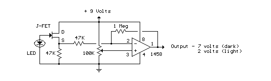
This circuit utilizes a JFET to receive signals from an LED and buffer them. The output voltage is managed using an IC 1458 or LM1458, which provides approximately 7 volts in darkness and experiences a drop of about 2...
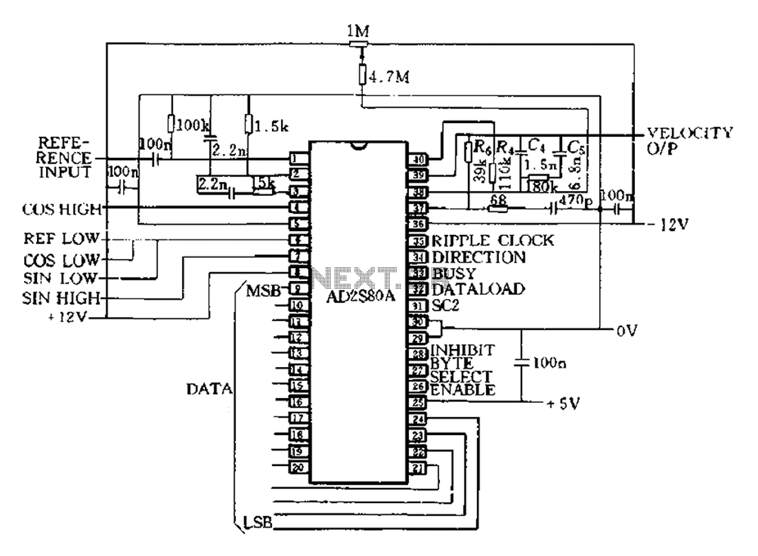
The AD2S80A represents a typical application circuit, detailing specific peripheral connectivity and device parameters. It is configured for a 12-bit resolution (SCl-0, Sc2 1) to select a reference frequency of 5 kHz. The bandwidth is 520 Hz, with a...
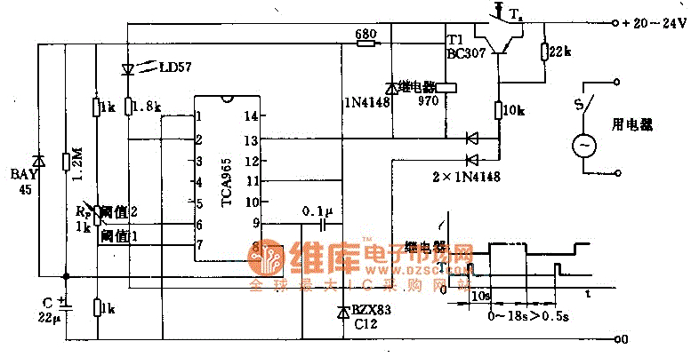
The foot 13 between valve value 1 and valve value 2 will draw the transistor base current. If the relay releases, after a recovery time of 0.5 seconds, pressing the key will initiate the switching process again. The timer...