
555 and 556 Timer Circuits

The trigger input activates when it drops below 1/3Vs (active low), resulting in a high output (+Vs). This input monitors the discharge of the timing capacitor in an astable configuration and possesses a high input impedance greater than 2M. The threshold input activates when it exceeds 2/3Vs (active high), causing the output to go low (0V). It monitors the charging of the timing capacitor in both astable and monostable circuits, with a high input impedance exceeding 10M. The reset input, when below approximately 0.7V (active low), forces the output low (0V), overriding other inputs. When not utilized, it should be connected to +Vs and has an input impedance of about 10k. The control input allows for adjustment of the internal threshold voltage, typically set at 2/3Vs. This function is seldom required, and it is common practice to connect the control input to 0V via a 0.01 µF capacitor to mitigate electrical noise. It may also remain unconnected if noise is not a concern. The discharge pin, while not an input, is included for convenience; it connects to 0V when the timer output is low, discharging the timing capacitor in both astable and monostable circuits.
The output of a standard 555 or 556 can sink and source up to 200mA, which exceeds the capabilities of most ICs, allowing it to directly power various output transducers, including LEDs (with a series resistor), low-current lamps, piezo transducers, loudspeakers (with a series capacitor), relay coils (with diode protection), and some motors (with diode protection). However, the output voltage does not fully reach 0V and +Vs, particularly under high current conditions. The capability to both sink and source current enables the connection of two devices to the output, so that one operates when the output is low while the other functions when the output is high. An example is illustrated with two LEDs connected in this manner, utilized in the Level Crossing project to create an alternating flash effect. A capacitor (approximately 100 µF) must be connected in series with the output of a 555 or 556 astable circuit when interfacing with speakers, as the output resembles a steady DC voltage of about ½Vs combined with a square wave AC (audio) signal. The capacitor blocks the DC component while allowing the AC signal to pass, a concept known as capacitor coupling.
Like all ICs, the 555 and 556 require protection from brief high-voltage spikes generated when an inductive load, such as a relay coil, is deactivated. A standard protection diode must be connected in reverse across the relay coil as shown in the schematic. Additionally, the 555 and 556 necessitate an extra diode connected in series with the coil to safeguard against voltage spikes. This protective measure ensures the longevity and reliability of the circuit in various applications.The 8-pin 555 timer must be one of the most useful ICs ever made and it is used in many projects. With just a few external components it can be used to build many circuits, not all of them involve timing! A popular version is the NE555 and this is suitable in most cases where a `555 timer` is specified. The 556 is a dual version of the 555 housed in a 14-pin package, the two timers (A and B) share the same power supply pins. The circuit diagrams on this page show a 555, but they could all be adapted to use one half of a 556. Low power versions of the 555 are made, such as the ICM7555, but these should only be used when specified (to increase battery life) because their maximum output current of about 20mA (with a 9V supply) is too low for many standard 555 circuits.
The ICM7555 has the same pin arrangement as a standard 555. The circuit symbol for a 555 (and 556) is a box with the pins arranged to suit the circuit diagram: for example 555 pin 8 at the top for the +Vs supply, 555 pin 3 output on the right. Usually just the pin numbers are used and they are not labelled with their function. Standard 555 and 556 ICs create a significant `glitch` on the supply when their output changes state.
This is rarely a problem in simple circuits with no other ICs, but in more complex circuits a smoothing capacitor (eg 100 µF) should be connected across the +Vs and 0V supply near the 555 or 556. Trigger input: when <1/3Vs (`active low`) this makes the output high (+Vs). It monitors the discharging of the timing capacitor in an astable circuit. It has a high input impedance >2M Threshold input: when >2/3Vs (`active high`) this makes the output low (0V)*.
It monitors the charging of the timing capacitor in astable and monostable circuits. It has a high input impedance >10M Reset input: when less than about 0. 7V (`active low`) this makes the output low (0V), overriding other inputs. When not required it should be connected to +Vs. It has an input impedance of about 10k Control input: this can be used to adjust the threshold voltage which is set internally to be 2/3Vs. Usually this function is not required and the control input is connected to 0V with a 0. 01 µF capacitor to eliminate electrical noise. It can be left unconnected if noise is not a problem. The discharge pin is not an input, but it is listed here for convenience. It is connected to 0V when the timer output is low and is used to discharge the timing capacitor in astable and monostable circuits.
The output of a standard 555 or 556 can sink and source up to 200mA. This is more than most ICs and it is sufficient to supply many output transducers directly, including LEDs (with a resistor in series), low current lamps, piezo transducers, loudspeakers (with a capacitor in series), relay coils (with diode protection) and some motors (with diode protection). The output voltage does not quite reach 0V and +Vs, especially if a large current is flowing. The ability to both sink and source current means that two devices can be connected to the output so that one is on when the output is low and the other is on when the output is high.
The top diagram shows two LEDs connected in this way. This arrangement is used in the LevelCrossing project to make the red LEDs flash alternately. ) may be connected to the output of a 555 or 556 astable circuit but a capacitor (about 100 µF) must be connected in series. The output is equivalent to a steady DC of about ½Vs combined with a square wave AC (audio) signal. The capacitor blocks the DC, but allows the AC to pass as explained in capacitorcoupling. Like all ICs, the 555 and 556 must be protected from the brief high voltage `spike` produced when an inductive load such as a relay coil is switched off.
The standard protectiondiode must be connected `backwards` across the the relay coil as shown in the diagram. However, the 555 and 556 require an extra diode connected in series with the coil t 🔗 External reference
Related Circuits
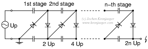
The Greinacher doubler circuit (a) transforms a grounded AC voltage (peak voltage Up) into symmetrical DC voltages of 1x Up each, thus producing 2x Up between outputs. If the input voltage is already symmetrical (e.g. as in an Obit),...
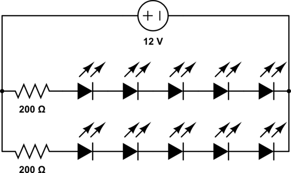
A 12V power supply is available, and there is a need to power LEDs with a forward voltage of 2V. It is questioned whether only six LEDs can be powered or if the cathode of one LED can be...
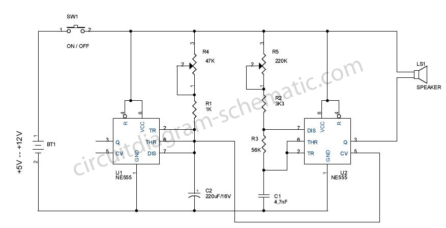
The tools used in this circuit are designed to create a noisy atmosphere. This circuit is relatively simple and is controlled by two 555 timer integrated circuits (ICs), assisted by other discrete components such as resistors and capacitors. The...
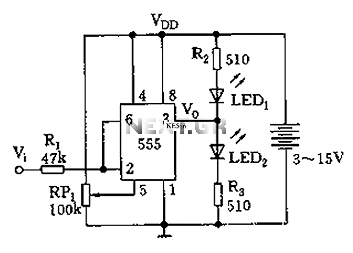
Figure 555 illustrates a simple logic circuit test lead. The test pen utilizes the 555 timer IC as its core component, incorporating a Schmitt trigger to assess the logic state of digital circuits. The circuit has two outputs: when...
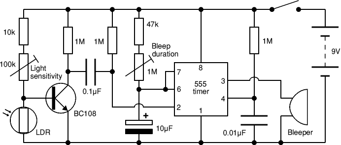
The function of this circuit is to detect a sudden shadow falling on the light sensor and to activate a buzzer when this occurs. The light sensor is designed to monitor ambient light levels. The circuit utilizes a light-dependent resistor...
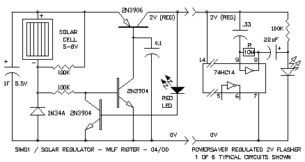
The PowerSaver Flasher uses capacitive output coupling to produce brighter shorter flashes and has a much lower average current drain than standard bicore or 74HC14 flashers. The PS Flasher with one LED circuit (2 LEDs) runs all night from...