
555 camera flash delay circuit

The camera flash delay circuit utilizes a light gate mechanism to accurately time the activation of the camera flash during rapid events. The luminous diode emits light that is detected by the 3DU photosensitive tube. In normal conditions, the photosensitive tube remains conductive, allowing current to flow through the circuit. However, when an object passes through the light beam, it casts a shadow on the photosensitive tube, leading to a sudden change in its conductivity.
This change generates a positive transition pulse that is sent to a transistor (VT2), which acts as a switching element in the circuit. The pulse triggers the 555 timer IC (IC1), configured in a monostable mode. Upon receiving the low-level pulse, the 555 timer initiates a timing cycle, which determines the duration of the flash. The output pulse from the 555 timer controls the flash mechanism, ensuring that the flash is activated for a very short duration, suitable for freezing motion in high-speed photography.
The circuit may also include additional components such as resistors and capacitors to fine-tune the timing characteristics and ensure proper operation of the 555 timer. The design allows for adjustments to be made, enabling the user to optimize the exposure time based on specific lighting conditions and the speed of the subject being photographed. Overall, this camera flash delay circuit is an effective solution for capturing fleeting moments with precision and clarity.As the figure 17-1 showns, the camera flash delay circuit can be used to capture the high-speed scene, and you can get a very short exposure time. The light door is composed of the luminous diode and the 3DU type photosensitive tube. When the light is shadowed, the positive transition pulse adds to the VT2. The IC1(555) is triggered by the low-level pulse, 5.. 🔗 External reference
Related Circuits
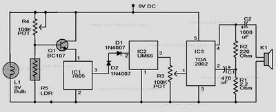
When there is no smoke, the light from the bulb directly illuminates the Light Dependent Resistor (LDR). In this condition, the resistance of the LDR is low, resulting in a voltage drop of less than 6V across it. Consequently,...
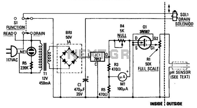
The drain-to-source resistance of Q1 varies depending on the acidity of the sample presented to Q1's gate circuit. This variable resistance influences the current flowing through the bridge, which is proportional to pH. The circuit involves a field-effect transistor (FET),...
The circuit utilizes a 555 timer configured as a multivibrator, where the oscillation frequency is determined by resistors R1, R2, and capacitor C1. The frequency formula is given by fo = 1.443 / ((R1 + R2) * C1). The...
The NE555 circuit implementation involves various connections and configurations. The circuit is designed with a supply voltage (Vcc) of +11V. The input terminal (pin 3) serves as a reset pin, and the relay and motor components are integrated into...
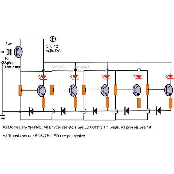
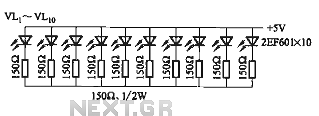
The LEDs in the circuit light up sequentially and "dance" in response to the music level applied at the input, preferably from the speaker terminals of the audio device being monitored. This configuration is consistent across all LEDs in...
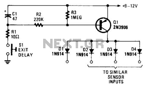
Depressing SI charges CI to the supply voltage. This biases Q1 on via bias resistors R2 and R3. A voltage is available for the duration of the delay period to hold off the alarm circuit. CI can be increased...