
555 DC Voltage Doubler Circuit

This DC voltage doubler circuit is designed to efficiently convert a lower input voltage into a higher output voltage, making it suitable for various electronic applications where increased voltage is necessary without the need for a separate power supply. The use of the LM555 timer IC as an astable multivibrator is instrumental in generating the required square wave signal, which is essential for the operation of the subsequent transistor stage.
The transistors T1 and T2 play a crucial role in the voltage doubling process by alternating their conductive states in response to the square wave signal. This switching action allows for the charging of capacitors C4 and C5, effectively stacking the voltages. The diodes D1 and D2 ensure that the current flows in the correct direction, preventing backflow and maintaining the charge in the capacitors.
The circuit's design emphasizes simplicity and efficiency, utilizing readily available components. The output voltage can reach up to 20 volts under no-load conditions, while the actual output voltage settles around 18 volts under load, demonstrating the effectiveness of the voltage doubling process. The specified maximum load of 70 mA ensures that the circuit operates within safe limits, maintaining reliability and longevity.
In applications where voltage stability is critical, integrating a voltage regulator IC at the output can enhance performance by providing a consistent output voltage despite variations in load or input voltage. However, it is essential to consider the additional current draw from the regulator to avoid exceeding the circuit's maximum current capacity. This careful consideration ensures optimal performance and reliability in practical applications.This dc voltage doubler circuit produces a voltage that is twice its voltage supply. This is useful when a higher voltage level is needed out of a single lower voltage power supply. Since the current consumption levels are low in such cases, the circuit can be built with minimal resources. The electronic circuit is basically a square wave generato r using the common LM555 timer IC. It is followed by a final stage made of transistors T1 and T2. The actual doubler circuit is made of D1, D2, C4 and C5 components. The 555 dc voltage doubler timer IC works as an astable multivibrator and generates a frequency of about 8. 5 kHz. The quare wave output drives the final stage made of T1 and T2. This is how the doubler works: by a low amplitude of the signal, transistor T1 blocks while T2 conducts.
The minus electrode of the capacitor C4 is grounded and charges through D1. By a high amplitude of the signal, transistor T1 conducts while T2 blocks. However, capacitor C4 cannot discharge because it is blocked by D1. The following capacitor C5 is therefore charged with a combined voltage from C4 and the power supply (12V input). On standby, the circuit delivers around 20 volts. The maximum load must not exceed 70 mA. The actual output voltage is around 18 volts giving an efficiency rating of 32 %. If a stable voltage lever is desired, a 3 pin voltage regulator IC can be added at the output. The regulator IC`s own current consumption must be added to the total current consumption which must not exceed 70 mA.
🔗 External reference
Related Circuits

When the door is opened, SW1 closes, powering the circuit and turning on the lamp. C1 begins to charge slowly through R1, and when the voltage at pins #2 and #6 of IC1 reaches 2/3 of the supply voltage,...

This circuit is a differential analog switch circuit utilizing the FM1208 monolithic dual differential multiplexer. It is designed for applications where the on-resistance (RDS(ON)) must match closely. The RDS(ON) for the monolithic dual multiplexer exhibits better than 1% accuracy...
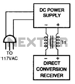
One solution for AC power line hum and ripple, which is caused by leakage current, is to utilize a well-regulated and filtered 9 to 18 VDC power supply that incorporates a balancing choke (Tl in this illustration) between the...
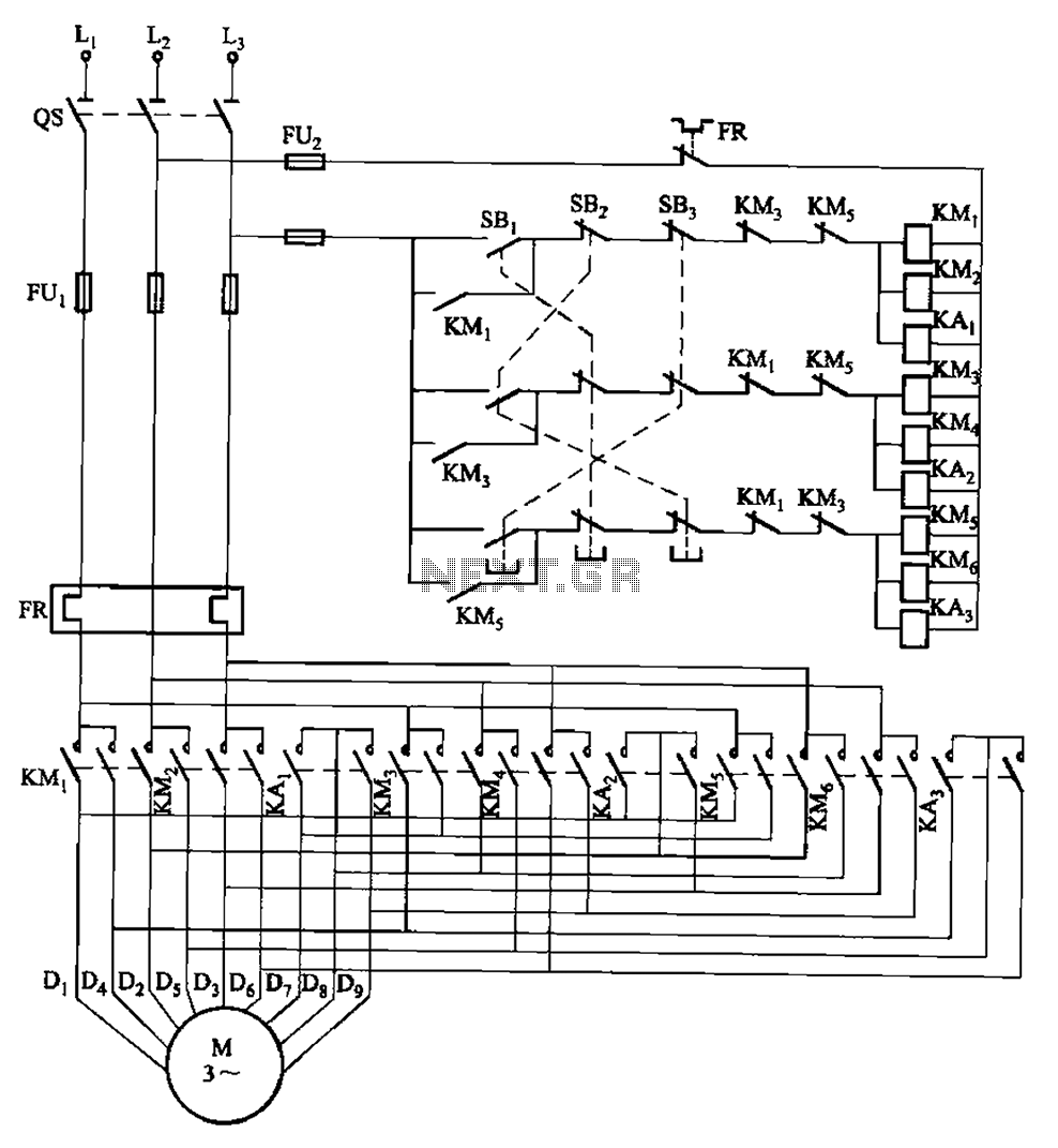
The circuit depicted in Figure 3-115 utilizes contactors and double buttons, allowing for speed conversion without the need to press the stop button. The buttons SBi, SBz, and SB3 correspond to high, medium, and low-speed operation, respectively. This circuit design...
VOX is a voice-activated switch commonly used with microphones as an alternative to traditional push-button switches. The VOX can be connected to various audio equipment featuring an external speaker for coupling. The activation threshold is adjusted using the volume...
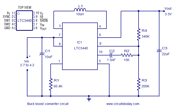
A highly efficient buck-boost converter circuit is presented, utilizing the LTC3440 buck-boost regulator IC from Linear Technology. This IC requires only one inductor and achieves efficiency levels of up to 96%. For applications where the output voltage is below...