
555-pin chip data and circuit diagrams

The 555 timer integrated circuit is widely used in applications requiring timing, oscillation, and pulse generation due to its reliability and versatility. The circuit can be configured in astable, monostable, or bistable modes, allowing for a variety of timing functions. In the astable mode, the 555 timer continuously oscillates, generating a square wave output. The frequency of oscillation and duty cycle can be adjusted by changing the values of the timing resistors and capacitors connected to the circuit. In the monostable mode, the 555 timer produces a single output pulse in response to a trigger input, with the duration of the pulse determined by the external resistor and capacitor values. The bistable mode allows for two stable states, functioning as a flip-flop that can be toggled between high and low states by applying triggers to the appropriate pins.
The 555 timer's internal design utilizes a combination of transistors for switching and amplifying signals, diodes for protecting against voltage spikes, and resistors for setting timing intervals. This structure enables the 555 timer to achieve high precision and stability across a range of operating conditions. The ability to operate at various voltages and output currents makes the 555 timer suitable for driving loads such as LEDs, motors, and relays, enhancing its utility in both hobbyist and professional electronic designs. The 555 timer remains a fundamental component in the field of electronics, often serving as an introductory device for learning about timing circuits and signal generation.Any time base circuit 555, the internal structure of the same circuit, the performance is the same. When there are many manufacturers base circuit 555 models, such as MC555, CA 555, XR555, LM555, etc; domestic models SL555, FX555,5G1555 etc. Typically, the most common is the letter NE555.555 former represents only manufacturers. Timebase circuit 555 is a wider use of precision timers can be used to pulse occurs, as square wave generator, self-excited oscillator, timing circuits, delay circuits, pulse-width modulation circuit, pulse width lack indicating circuit monitoring circuit. The operating voltage is 5 ~ 18V, commonly 10 ~ 15V, maximum output current 200mA, can drive the power switch, relay, LED, LED, doing oscillator, the highest frequency up to 300kHz.
555 time base circuit is relatively simple, the internal integration transistor 21, four crystal diodes and 16 resistors, two voltage comparators, an RS flip-flop, a transistor and a resistor from the three discharge voltage divider. FIG comparator A1 and comparator A2 is lower by two high-gain voltage comparator, VT for the discharge transistor, three resistors R1, R2, R3 resistance is 5k, 3 5 is composed of the time base circuit 555 name of the resulting.
555 8-pin integrated circuit operating voltage input terminal voltage is 5 ~ 18V, with UCC represents; seen from the divider, comparator A1 of 5 feet between R1 and R2, so the voltage is 5 feet fixed on 2UCC/3; comparator A2 is connected between R2 and R3, with the potential of the inverting input of A2 is fixed to the UCC/3. 1 foot to ground. 2 feet for a trigger input; the output of 3 feet, the level of state control output by the flip-flop, and the flip-flop by the comparator 6 feet and 2 feet at a relatively controlled.
When the trigger on the high acceptance of the comparator A1 from R pin input, triggers are placed in the reset state, 3 feet output low; 2 feet and 6 feet are complementary, only 2 feet of low-level work, the high level it does not work, that voltage is less than 1Ucc/3, 3 feet high output at this time. 6 feet for the end of the threshold, only the high work, low it does not work, the input voltage is greater than 2 Ucc/3, said the high end of the trigger, 3-pin output low, but there is a precondition, That potential must be greater than 2 feet 1Ucc/3 when effective.
3 feet high potential close to the supply voltage Ucc, the maximum output current to play 200mA. Reset terminal 4 feet, 4 feet when the potential is less than 0.4V, regardless of the status of 2,6 feet, the output of 3 feet output low. 5 feet control terminal. 7 feet, said discharge end, and 3-pin output synchronous output level consistent, but not 7 feet output current, so called solid 3 feet high (or low), 7 feet called unrealistically high.
Related Circuits
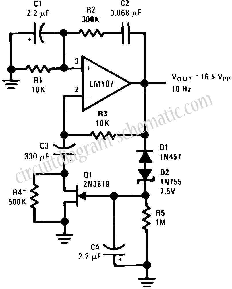
This circuit eliminates the traditional tungsten filament lamp amplitude regulator along with its associated time constant and linearity issues. Additionally, it addresses the reliability problems commonly found with lamps. The Wien Bridge oscillator is utilized, leveraging the fact that...
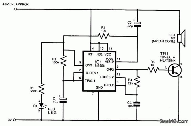
An adaptable siren generator circuit with multiple applications is presented. It is based on a 556 twin-timer chip, IC1. One timer section generates an audio tone that is directly coupled to the driver transistor, TR1. The other half of...
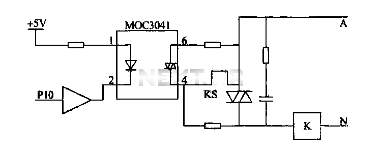
Device for an intermediate relay. The circuit utilizes a Triac AC contactor interface, employing the MOC3041 Triac output optical coupler to trigger the Triac. When Pl0 is low, the Triac will be activated, energizing the AC contactor coil. The described...

The impedance linear amplifier circuit is illustrated in FIG 75 and is configured using the RF2320 component. Connectors J1 and J2 are 75-ohm connectors. The impedance linear amplifier circuit designed with the RF2320 is intended for applications requiring high fidelity...
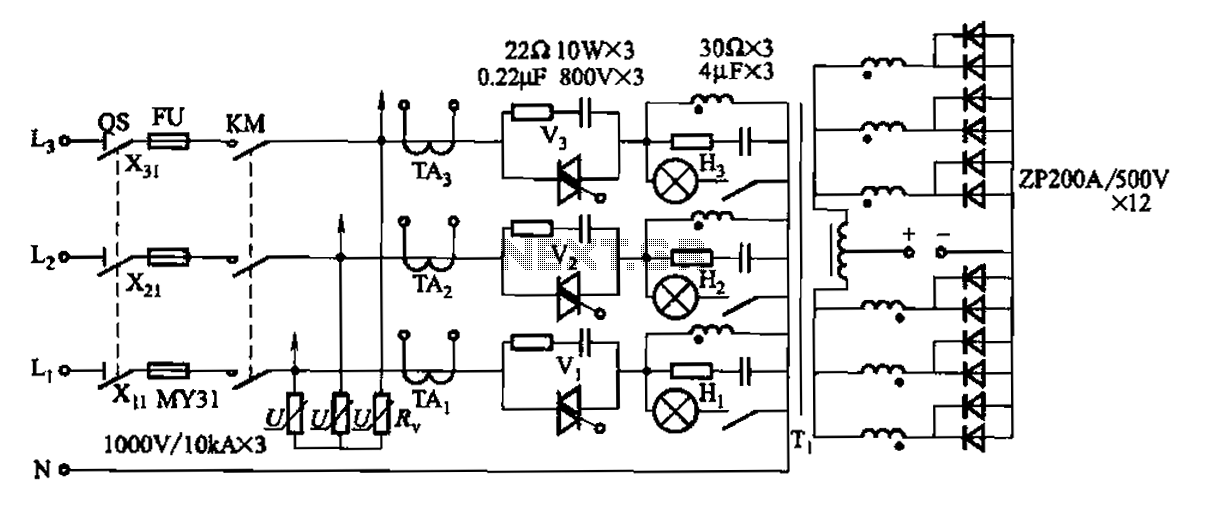
A 1500A-7V phase thyristor power regulator circuit is designed for plating applications. It consists of three major components: the main circuit, the control circuit, and the protection circuit. The control circuit includes a trigger circuit, a synchronous power supply,...

The output voltage can be calculated as follows: U = 1.3 (1 + R3 / R4) (V), where R3 and R4 are part of an adjustment potentiometer, allowing for a continuously adjustable output voltage. The described circuit involves a voltage...