
A TREAD sized regulator

The schematic design is characterized by a compact layout, measuring 5 cm by 3.3 cm, which is conducive to efficient circuit performance. The foundational principles drawn from Walt Jung's work emphasize noise reduction and line rejection, critical factors in the design of voltage regulators. The modifications applied to the original design reflect a thoughtful approach to enhancing performance based on established methodologies.
The layout considerations prioritize low noise, necessitating specific alterations to the ground connections. The recommendation to sever the fat ground track between the diode bridge and output connector and to establish a new track from the ground of capacitor C2 is crucial. This change aims to isolate the clean ground path from the noisy ground associated with D2 and C2, thereby reducing potential interference in the circuit's performance.
Incorporating an RC filter immediately following the diode bridge serves to dampen high-frequency switching transients, thereby further enhancing the stability of the output voltage. The choice of resistor values in the RC filter is instrumental in achieving the desired noise reduction.
The design of Q6 requires careful consideration regarding noise performance. While a resistor may provide a straightforward solution, assessing the noise characteristics of the chosen components is essential for optimizing the overall circuit performance. The use of a dual resistor and capacitor combination (R5 and C3) is a strategic choice to minimize leakage current noise, which can be detrimental to the filter's efficacy.
Output current limitations are determined by the current source characteristics of Q2 and the hFE of the selected pass transistor. The proposed use of a J202 transistor, with its specified Idss range, alongside a D44H11 pass transistor, provides flexibility in achieving the desired current output. The option to use a J203 transistor allows for potential increases in current limits, accommodating varying application requirements.
Overall, the schematic reflects a robust design approach, integrating established principles with practical modifications aimed at optimizing performance and reliability in voltage regulation applications.The size of the tread was 5cm by 3cm. My design, at the moment is 5cm by 3. 3cm. The basis of the regulator is taken from Walt Jung`s 1997 article Regulator Excels In Noise and Line Rejection. With a few changes based upon other Walt Jung articles on constant current sources and buffered voltages references, the schematic was born:
At this moment, I looking for comments either on the schematic or the layout before I send it out for prototypes. I`m hoping that the layout should be fairly low noise. - the fat ground track in between the diode bridge and the output connector must be cut and replaced by a track starting at C2 ground.
Nothing should be connected in between D2 and C2, it`s your dirtiest ground. - If you don`t mind being wasteful, a RC filter just after the diode bridge (something like 5-10 ohms before your first cap) quiet down the switching transients. - Q6 - a resistor might work, but then again which is quieter By designing for Q6, you can always build cheap with a resistor, but the other way around is harder.
- R5, C3 - the dual resistor and cap combination is to reduce leakage current noise in the filter (taken from here: and I`ve seen in a few other places as well) what`s your current output limit based on the pass transistor i presume. also fixed voltage out one of the beauties of the lm317/lt108x circuits is some voltage adjustment. A trimmer between r3 and ground It is fixed out. But the question I would ask is how ofter do you actually change voltage of a built supply I will take a look at sizing to put a trimmer there.
The other side of that though is that because the op-amp is powered from the regulated rail, some trim positions could end up in dis-functional regulator. As for current output, the limit would be CCS current of Q2 times by the hfe of the pass transistor. I`m thinking of a J202 (Idss of 0. 9 - 4. 5ma) and a D44H11 as the pass (which looking at the curves seems to be about 125 as hfe). So part selection determines the ultimate current limit. The J202, could be replaced with J203 for higher limits. It is fixed out. But the question I would ask is how ofter do you actually change voltage of a built supply I will take a look at sizing to put a trimmer there.
The other side of that though is that because the op-amp is powered from the regulated rail, some trim positions could end up in dis-functional regulator. As for current output, the limit would be CCS current of Q2 times by the hfe of the pass transistor. I`m thinking of a J202 (Idss of 0. 9 - 4. 5ma) and a D44H11 as the pass (which looking at the curves seems to be about 125 as hfe). So part selection determines the ultimate current limit. The J202, could be replaced with 🔗 External reference
Related Circuits
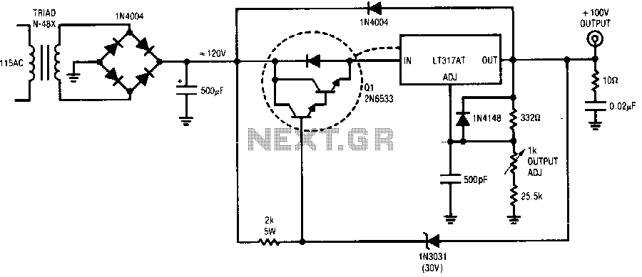
The regulator provides a 100 V output at 100 mA and can withstand shorts to ground. Even at a 100 V output, the LT317A operates in normal mode, maintaining a 1.2 V difference between its output and adjustment pin....
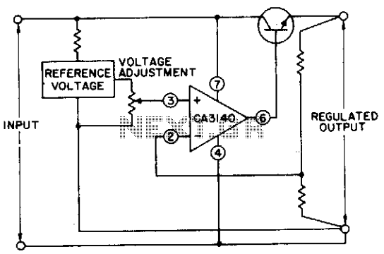
The circuit utilizes a CA3140 BiMOS operational amplifier that is capable of providing a regulated output adjustable from approximately 0 to 24 volts. The circuit is fully regulated. The CA3140 BiMOS operational amplifier is a versatile component that combines the...
The project encompasses both hardware and software design for a 12/24V DC 20A charge controller suitable for solar, wind, hydro, or pedal power applications. This initiative aims to create an open-design, cost-effective, yet fully functional charge regulator for renewable...
The circuit is designed to charge a 12-volt component selection at a maximum current of six amperes. Once the battery voltage reaches its fully charged level, the SCR shuts off, and a trickle charge, determined by the resistance value...
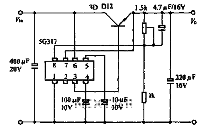
The 5G317 is an integrated voltage regulator circuit used in wiring applications for televisions. The maximum input voltage for the 5G317 should be less than 25V, while the output voltage ranges from 10V to 18V. The maximum output current,...
The Arduino is a user-friendly and versatile controller platform suitable for various projects. Recently, an Ethernet shield was purchased for the Arduino to enable remote control of projects, which proved to be highly effective. This led to the idea...