
Ac-to-DC converter

The described circuit employs a PMOS enhancement-mode field-effect transistor (FET) as an input buffer amplifier. This type of FET is characterized by its ability to operate with a positive gate-source voltage, which enhances its conductivity. The input buffer configuration serves to isolate the input signal from the subsequent circuitry, ensuring that the input impedance remains high while the output impedance remains low. This arrangement is particularly beneficial in applications where signal integrity and impedance matching are crucial.
The absolute value circuit is designed to convert both positive and negative input signals into a positive output. This is achieved through the use of diodes D1 and D2, which are arranged in a way that allows for the conduction of the signal regardless of its polarity. By incorporating these diodes, the circuit effectively eliminates the forward voltage drop that typically occurs when diodes are conducting. This is significant because the forward voltage drop can introduce inaccuracies in the output signal, particularly in precision applications.
In summary, the combination of the PMOS enhancement-mode FET input buffer and the absolute value circuit allows for a robust design that maintains signal integrity while providing accurate output levels, regardless of the input signal's polarity. This circuit configuration is well-suited for use in various electronic applications where accurate signal processing is essential.This circuit includes a PMOS enhancement-mode FET input buffer amplifier, coupled to a classical absolute value circuit which essentially eliminates the effect of the forward voltage drop across diodes D1 and D2.
Related Circuits
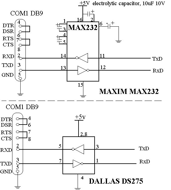
A standard serial interfacing for PC, RS232C, requires negative logic, i.e., logic 1 is -3V to -12V and logic 0 is +3V to +12V. To convert a TTL logic, say, TxD and RxD pins of the uC chips, thus...

The current circuit is designed to convert sinusoidal input signals into TTL output signals. It is capable of handling input signals greater than 100 mV and operates effectively at frequencies up to approximately 80 MHz. Transistor T1 is configured...

This application note presents the component values and measured performance for the MAX2681 mixer IC when tuned for GPS operation at 1575 MHz. The MAX2681 is a high-performance mixer integrated circuit designed for use in GPS applications, particularly at the...
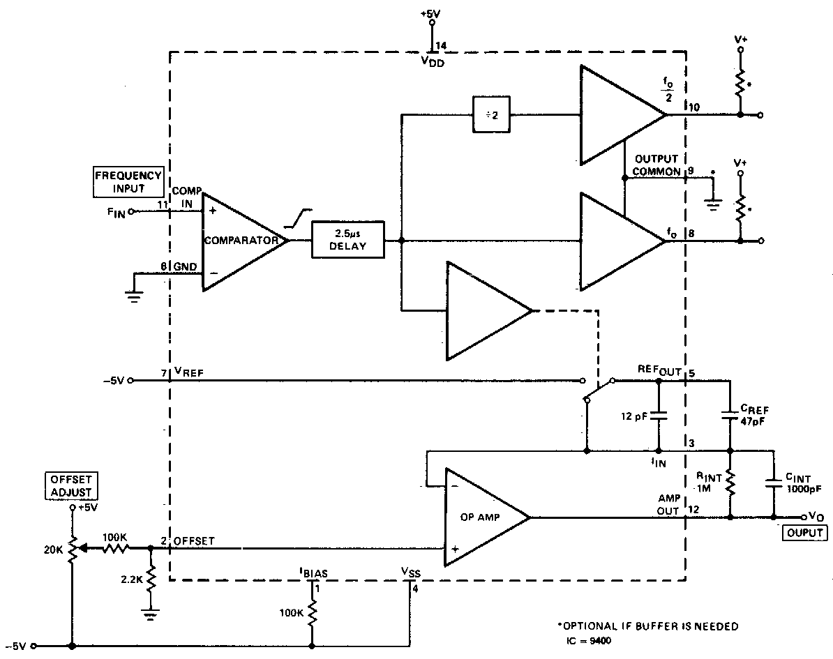
The converter produces an output voltage that is linearly proportional to the input frequency waveform. Each zero crossing at the comparator's input results in a specific change being dispensed into the op-amp's summing junction. This charge subsequently flows through...
This project originated from an interest in a new form of radio transmission known as Digital Radio Mondial (DRM). The Digital Radio Mondial (DRM) is a revolutionary digital broadcasting technology designed for AM and FM radio. It provides enhanced audio...

The pressure transmitter circuit data acquisition system utilizes the 1B31, an 18-bit A/D converter (AD1170), and an MCS-51 microcontroller. The configuration, as depicted in the accompanying diagram, features a full-scale output voltage of 10 mV from the pressure transmitter...