
ADF4158 PLL strange moving spurs

The circuit described involves a TCXO (Temperature Compensated Crystal Oscillator) operating at a fundamental frequency of 10 MHz, which is critical for precision timing applications. The phase noise performance of the TCXO is superior to that of the HP8562E spectrum analyzer, indicating a high-quality oscillator that minimizes jitter and improves signal integrity. The presence of measurable harmonics up to 2-3 GHz suggests that the TCXO can maintain signal purity across a wide frequency range, which is essential for applications requiring stable and accurate frequency generation.
The TCXO's slew rate, measured at approximately 2.5-3 ns/V, indicates its ability to transition between voltage levels, which is crucial for maintaining signal fidelity in high-speed applications. The measurement of 400 V/μs meets standard requirements, ensuring that the output can drive subsequent stages effectively. The exploration of using an ECL (Emitter Coupled Logic) gate to interface between the TCXO and the ADF (Analog Digital Frequency Synthesizer) highlights a potential strategy for improving output phase noise by providing better drive capability and reducing signal degradation.
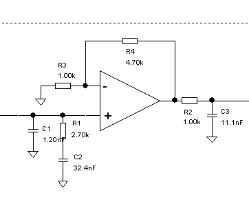
The reference pin on the op-amp is derived from P3VA and utilizes a bridge resistor, ensuring a stable reference voltage. The modification from a ground connection to this configuration indicates a design evolution aimed at enhancing performance. The addition of a capacitor to this reference pin can further stabilize the voltage and reduce noise, which is crucial for maintaining the integrity of the PLL (Phase-Locked Loop) operation.
The layout of the PCB, with short tracks and minimized grounding, is a critical consideration in high-frequency designs to prevent unwanted inductance and capacitance that can adversely affect performance. The use of a single ground plane in a mixed-signal environment poses challenges, as it can lead to interference between clean and dirty signals. The designer's efforts to separate these signals through strategic placement are commendable, but further improvements may be necessary to ensure optimal performance, particularly in high-frequency applications where noise and signal integrity are paramount. Measurements taken on the P3VA side are not mentioned, suggesting that further analysis in that area may be warranted to fully understand the system's performance.On the 10 MHz fundamental I only measure the HP8562E PN flloor meaning that the TCXO phase noise is better than the spectrum analyzer noise floor. I`ve measured some harmonics from 20 MHz to 1 GHz. There are still measurable harmonics up to 2-3 GHz. 2. TCXO Slew rate have been measured at about 2. 5~3ns/V = 400V/us which is the minimum requirement or slightly lower. I`ve tried different sources without any change in the output phase noise. An improve might be to use an ECL gate for instance between the TCXO and the ADF to drive the REFin, right 4. apprently yes the ref pin on the opamp seems clean. It`s derived from P3VA with a bridge resistor. This is a modification brought on the prototype as the schematic above show a connection to GND. I`m going to add a capacitor on it to improve if needed. 5. Figure below is the PLL chip on top and the OP184 on bottom. tracks are short, grounding made as short as possible. On things which might be improved, the PCB which contains mixed parts has one GND plane only. I`ve tried to ensure that dirty and clean signals do not mix by locating them properly, but this could indeed be not enough.
But I do not measure things on P3VA side. 🔗 External reference
Related Circuits

All components used in the Moving Sensor/Detector Schematic Diagram utilize the IC NE555 and the Phototransistor L14F. The primary component in this circuit is the IC NE555, along with an IR LED, the Phototransistor L14F, and the IC LM1458....
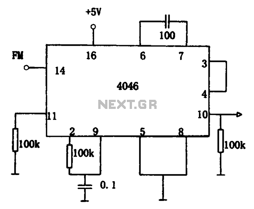
The circuit utilizes the 4046 Phase-Locked Loop (PLL) for FM demodulation, incorporating an intermediate frequency (IF) FM demodulation output based on the input signal frequency. The 4046 PLL is a versatile integrated circuit that can be configured for various applications,...
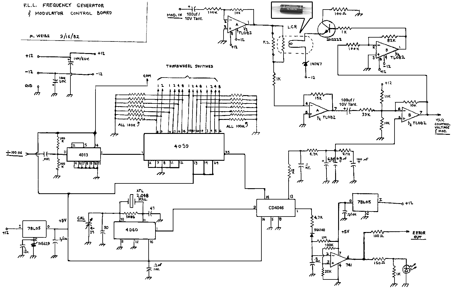
This is a Phase-Locked Loop (PLL) controller designed to operate with a Voltage-Controlled Oscillator (VCO) and modulator. These two modules should be utilized together to create a complete baseband-capable exciter unit. The PLL controller incorporates a stable crystal-controlled reference...
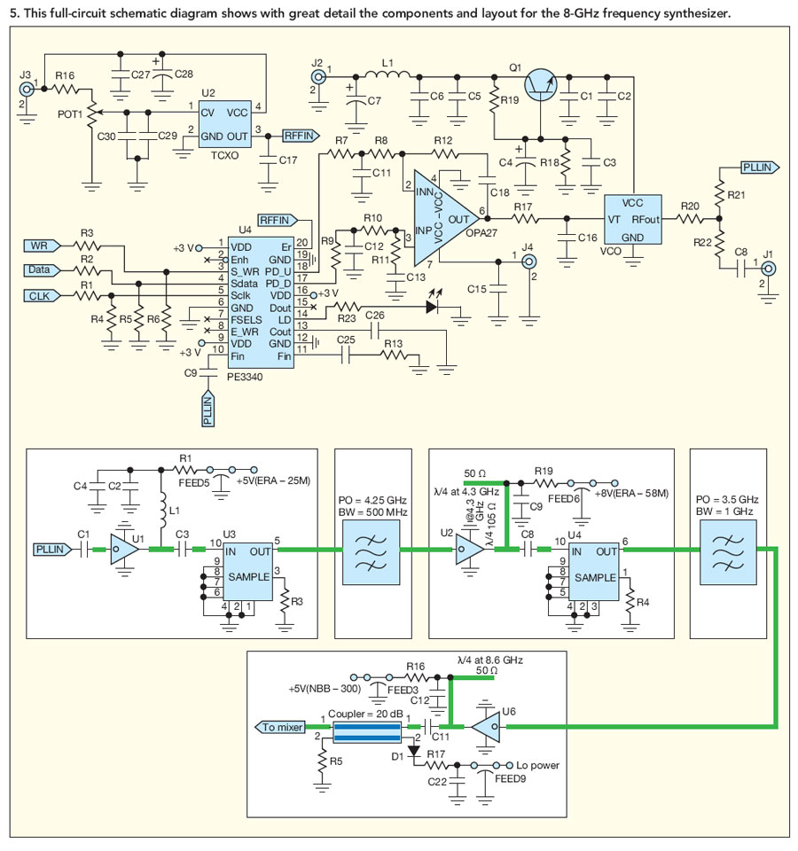
Designing a Phase-Locked Loop (PLL) synthesizer for modern mobile communication systems requires achieving the right balance among several trade-offs, including spurious levels and frequency switching speed. The design of a Phase-Locked Loop synthesizer for mobile communication systems is a critical...
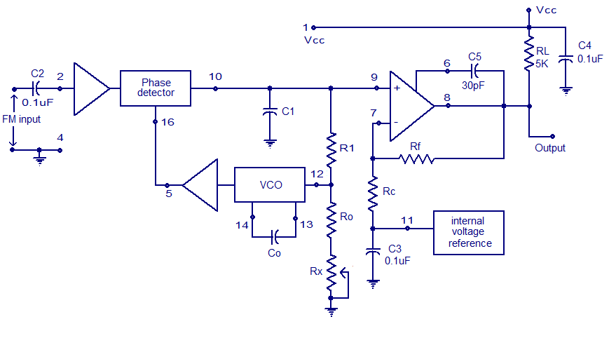
A simple PLL FM demodulator circuit using the IC XR2212 is presented. The XR2212 is a highly stable, monolithic PLL (phase-locked loop) IC specifically designed for communication and control system applications. It operates within a frequency range of 0.01...
A problem has been encountered in a Phase-Locked Loop (PLL). A loop filter has been utilized, but the output spectrum does not meet expectations. In a Phase-Locked Loop (PLL) system, the loop filter plays a crucial role in determining the...