
ADUC832 1.3MIPS 8052 MCU + 62kB Flash + 8-Ch 12-Bit ADC + Dual 12-Bit DAC

The ADUC836 MicroConverter represents a significant advancement in integrated data acquisition systems, combining the functionality of analog-to-digital (A/D) and digital-to-analog (D/A) conversion along with a microcontroller in a single package. This integration facilitates compact design solutions for applications requiring precise data processing and control.
The device's compatibility with the ADuC816 ensures a smooth transition for users upgrading from previous models, minimizing the need for redesign efforts. The availability of both 52-pin PQFP and 56-pin CSP packages provides flexibility in design, allowing engineers to select the optimal footprint for their specific application needs.
Operating on a dual voltage of 3V or 5V enhances the versatility of the ADUC836, making it suitable for a wide range of applications, from battery-powered devices to more robust systems. The use of a 32 kHz crystal oscillator, paired with an on-chip phase-locked loop (PLL), enables the generation of a stable high-frequency clock at 12.58 MHz, which is essential for maintaining precise timing in data acquisition processes.
The programmable clock divider further enhances the device's flexibility, allowing designers to tailor the microcontroller core clock frequency to meet the requirements of their application. The 8052 core architecture ensures that existing 8051 code can be utilized without modification, thus streamlining development processes and reducing time-to-market.
In summary, the ADUC836 MicroConverter is a powerful and versatile solution for modern data acquisition needs, providing high precision, backward compatibility, and a range of operational features that cater to diverse electronic applications.The ADUC836 MicroConverter is a fully integrated 16-bit data acquisition system-on-a-chip. Like all of ADI`s MicroConverter products, it features precision A/D & D/A conversion and a Flash Microcontroller on a single chip. The ADUC836 is 100% backward compatible (hardware and software) with the ADuC816. It is available in 52-pin PQFP or 56-pin CSP packages and operates on a 3V or 5V power supply. The device operates from a 32 kHz crystal with an on-chip PLL generating a high frequency Clock of 12. 58 MHz. This Clock is routed through a programmable Clock divider from which the MCU core Clock operating frequency is generated.
The Microcontroller core is an 8052 and therefore 8051 instruction set compatible with 12 core Clock periods per machine cycle. By Analog Devices, Inc. 🔗 External reference
Related Circuits
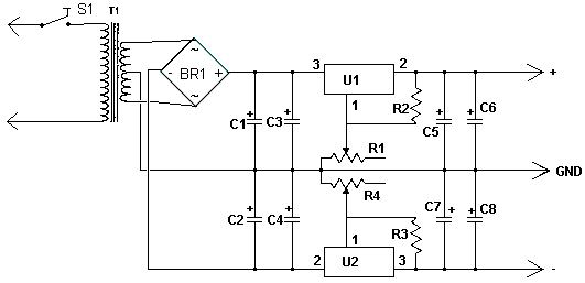
This dual polarity power supply is simple to construct, requires minimal components, and is adjustable from 0 to 15 volts. It is suitable for powering operational amplifier circuits as well as other circuits that necessitate a dual supply voltage....
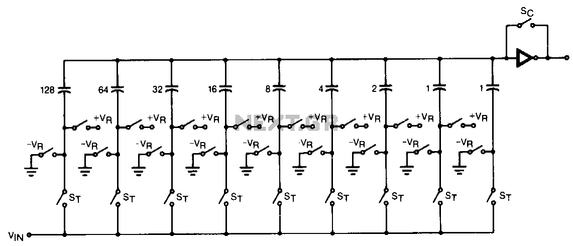
The CMOS comparator in the successive-approximation system determines each bit by examining the charge on a series of binary-weighted capacitors. In the first phase of the conversion process, the analog input is sampled by closing switch SC and all...
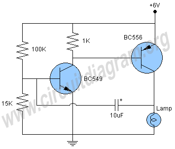
This is a simple two-transistor lamp flasher circuit that can be used to flash a 6-volt lamp. The circuit is compact and can be easily fitted into a small enclosure. It utilizes two transistors: one is an NPN BC549,...
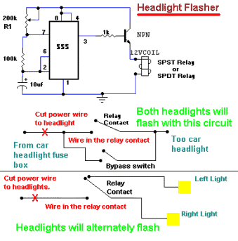
A compact and intriguing circuit designed to flash automotive headlights. The circuit diagram is based on the well-known NE555 timer circuit. This circuit utilizes the NE555 timer in astable mode to create a flashing effect for automotive headlights. The primary...
The YD9088 is a bipolar integrated circuit designed for use in mono portable and pocket radios. It is advantageous when minimizing peripheral components, which should be of small dimensions and low cost, is a priority. The circuit incorporates a...
The FM497 is an integrated electronic ignition controller designed for breakerless ignition systems that utilize Hall effect sensors. This device operates an external NPN Darlington transistor to manage the coil current, thereby delivering the necessary stored energy while maintaining...