
Analog 5Gb/s Clock-and-Data Recovery Circuit

The phase detector samples the data using three parallel master-slave flip-flops constructed with current-mode logic (CML) latches. One latch samples the data on the rising edge of the in-phase clock, another on the rising edge of the quadrature clock, and the last on the falling edge of the in-phase clock. A synchronization latch ensures that all paths are synchronized to the same clock edge. The two CML XOR gates detect the phase difference between the sampled data, generating the differential up and down pulses. The PI controller takes as input the two control currents produced by the voltage-to-current converter, I1 and I2. These currents are mirrored multiple times for various functions: (1) to be output directly as steering currents for the two phase interpolators; (2) to be compared by measuring the voltage drop across two identical resistors; (3) to be summed to produce the additional steering currents, I3 and I4. Digital control bits b1p, b1n, b2p, and b2n are generated by two comparators that determine the larger of the two pairs of PI controller currents. The first comparator evaluates the voltage drop across the resistors driven by I1 and I2, while the second compares the drops produced by I3 and I4. The outputs of the differential comparators are fed back to the PI controller as the aforementioned digital control bits.
Two phase interpolators are responsible for interpolating the phase of the local four-phase clock, resulting in the generation of the recovered four-phase clock. The extent of interpolation is contingent upon the magnitude of the four steering currents generated by the PI controller, adhering to the relationship: I1 + I2 = I3 + I4. Each phase interpolator consists of four resistively-loaded differential pairs, with currents directed to two nodes by the local clock. One phase interpolator generates the in-phase clock, while the other produces the quadrature clock by altering the sequence of the input currents. The CDR floorplan illustrates that the high-speed noisy blocks are powered by a separate VDD supply from the quieter blocks, indicating a strategic grouping. The feedback nature of the CDR complicates linear signal flow, necessitating specific signal management strategies.A clock-and-data recovery (CDR) circuit is used to both recover the clock from a transmitted data stream and re-time that data with the recovered clock. Such circuits are typically placed at the front-end of receiver chips to recover the clock from data sent from a transmitter chip across a backplane or other channel.
This project presents a fully -analog CDR that uses phase interpolation to adjust the phase of a locally generated 5GHz clock to align with the phase of an incoming 5Gb/s data stream. A binary phase detector performs two functions: (1) re-times the incoming data stream with the recovered clock; (2) compares the phase of the data and recovered clock, generating differential up and down pulses.
These pulses are converted to DC values by a differential charge pump and loop filter. A voltage-to-current converter converts these voltages to differential currents that fed to a phase interpolator (PI) controller. The PI controller determines the smaller of the two currents using a comparator and generates four steering currents.
These currents are fed to two phase interpolators and control the degree of interpolation applied to the four-phase (i. e. , differential in-phase and quadrature) locally-generated 5GHz clock. These phase-adjusted clocks are then buffered and fed back to the phase detector as the 5GHz recovered clocks, thereby completing the feedback loop.
A block diagram of the CDR is shown in Fig. 1. By adjusting only the local clock`s phase (and not its frequency), all data channels in a receiver can share a single PLL, thus significantly reducing area and power consumption. The phase detector, shown in Fig. 2 samples the data using three parallel master-slave flip-flops constructed with current-mode logic (CML) latches, one of which is shown in Fig.
3. The top path samples the data on the rising edge of the in-phase clock, the middle on the rising edge of quadrature clock, and the bottom on the falling edge of the in-phase clock. The third latch in the top two paths synchronizes all paths to the same clock edge. The two CML XORs, one of which is shown in Fig. 4, detect the phase difference between the sampled data and generate differential up and down pulses.
The phase interpolator (PI) controller, shown in Fig. 5, takes as input the two control currents generated by the V-I converter, I1 and I2. These currents are mirrored multiple times to (1) be output directly as steering currents for the two phase interpolators (PIs); (2) be compared by comparing the voltage drop developed across two identical resistors; (3) be summed to generate the other two steering currents, I3 and I4. The control bits b1p, b1n, b2p and b2n are digital control bits generated by two comparators. Two comparators determine the larger of the two PI controller current pairs. The first compares the drop developed across two resistors by I1 and I2, while the other compares the drops developed by I3 and I4.
The differential comparator outputs are fed back to the PI controller as the digital control bits described above. The comparator schematic is shown in Fig. 6. Two PIs interpolate the phase of the local four-phase clock and generate the recovered four-phase clock.
The degree of interpolation depends upon the magnitude of the four steering currents generated by the PI Controller, which obey the following relationship: I1 + I2 = I3 + I4. Each PI consists of four resistively-loaded differential pairs whose currents are steered to two nodes by the local clock.
One PI generates the in-phase clock while the other generates the quadrature clock by switching the order of the input currents. The PI schematic is shown in Fig. 7. The CDR floorplan is shown below in Fig. 25. The noisy high-speed blocks are powered by a separate VDD supply than the quiet blocks and hence were grouped together.
The feedback nature of the CDR prevented a linear signal flow and thus dictated that some signals 🔗 External reference
Related Circuits
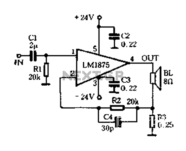
A current-sense amplifier is utilized to enhance the performance of the LM1875 current-mode amplifier circuit, as depicted in Figure 5-20. The resistor R3 and the series resistance of the speaker contribute to the current flowing through R3. This current...
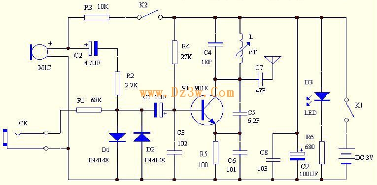
C4 and L form a resonator, where the resonant frequency corresponds to the FM transmitting power of the microphone. According to the component parameters in the diagram, the transmission frequency can range from 88 to 108 MHz. The frequency...
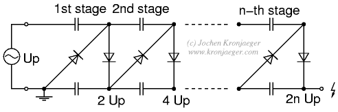
The Greinacher doubler circuit (a) transforms a grounded AC voltage (peak voltage Up) into symmetrical DC voltages of 1x Up each, thus producing 2x Up between outputs. If the input voltage is already symmetrical (e.g. as in an Obit),...
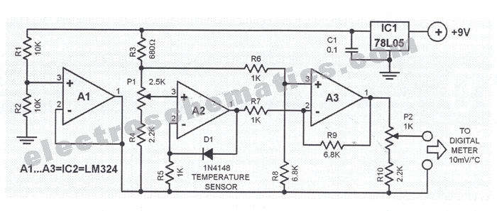
The circuit presented is designed to prevent burning one's tongue by monitoring the temperature of coffee. It consists of a voltage regulator, a temperature-to-voltage converter, a comparator, and two LEDs. In general, the circuit operates as follows: if the...

A preamplifier in the audio frequency range amplifies a noisy audio signal to drive a diode clipper. Suitable audio input levels would be in the 10-mV to 1-V range. The audio preamplifier circuit is designed to enhance weak audio signals, typically...
This document provides an overview of a simple circuit diagram for frequency (F and V) voltage conversion. It describes a digital frequency meter circuit primarily based on the LM555 timer IC, which is commonly used in various applications, including...