
Using current feedback amplifier circuit of LM1875

A current-sense amplifier is designed to accurately monitor and amplify the current flowing through a load, which in this case is a speaker. The LM1875 integrated circuit is configured in a current-mode setup to leverage its high performance for audio applications. The resistor R3, placed in series with the speaker, serves as a sensing element, allowing the amplifier to derive a proportional voltage that reflects the current through the speaker.
The feedback loop formed by resistor R2 is critical for maintaining the stability and accuracy of the amplifier. This feedback mechanism ensures that the output voltage corresponds accurately to the sensed current, which is essential for applications requiring precise current measurements. The use of negative feedback enhances the amplifier's output impedance, which is beneficial in maintaining signal integrity across varying load conditions.
Capacitor C4 is implemented for lead compensation, which helps to stabilize the amplifier and mitigate potential oscillations that can arise due to phase shifts in the feedback loop. Although R2 does not completely feedback the output current to the negative input, it plays a vital role in preventing detrimental effects from excessive feedback, thus ensuring the circuit operates within safe parameters.
The balancing of the positive and negative input bias terminals is crucial for eliminating any DC offset at the output, which could otherwise distort the amplified signal. The initial setup involves connecting two small resistors of 0.22 ohms to ground, establishing a reference point for the circuit. The grounding resistance is kept at approximately 6 ohms to maintain consistency in the measurements.
During the assembly process, the 24V power supply line and output line are soldered directly to the input terminals, allowing for efficient power delivery to the amplifier. A short circuit is created at the welding position of the loudspeaker resistance for testing purposes, enabling verification of the output voltage. The design ensures that the output voltage remains stable and below 100mV offset, confirming the amplifier's reliability over extended operation periods. After confirming the proper functioning of the circuit, the input can be disconnected, and speakers can be connected for normal operation.Current-sense amplifier to listen better t use amplifier IC LM1875 current-mode amplifier circuit shown in Figure 5-20. FIG resistor R3 and the speaker BL series resistance t i s small, the speaker of the current flowing through the flow through R3. In its sampling generated across the feedback input through R2 forming a voltage on the output feedback voltage proportional to the current in R3 amplifier end, the composition of the current negative feedback, the amplifier output impedance rises t while reducing damping circuit © the network canceled the so-called Joubert, only C4 for lead compensation. R2 is provided, although then the output current is not fully feedback to the negative input of the feedback, but indeed preventing stop the harmful effects of the large amount of feedback inputs generated; t the same time also make the positive and negative input bias terminal balanced to eliminate output terminal DC offset.
On the first, feet two small welding 0. 22 r -JI; F capacitance to their other end welded together as ground resistance grounding of about 6, are bent after welding at this point. 24V power supply line and the output line soldered directly related to the input terminals of the feet daily exchange of short circuit in a welding position the loudspeaker BL ion resistance, power testing ground output voltage 9 as described later, and less than half an hour almost no lOOrnV offset, you can disconnect the input shorting t connect speakers to.
Related Circuits
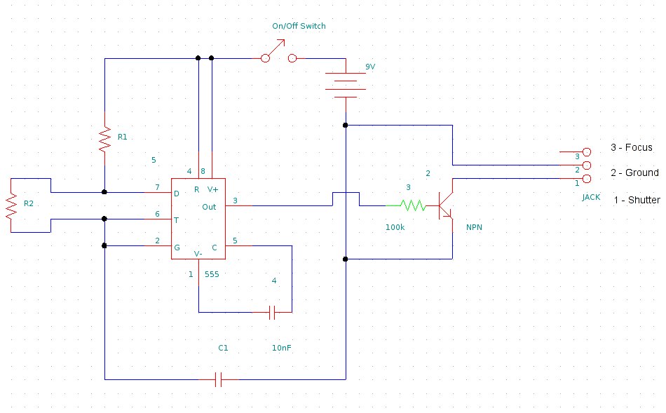
This document provides information on constructing a DIY time-lapse circuit that enables a camera to automatically capture images at specified time intervals. These images can then be compiled to create a time-lapse film. The circuit utilizes a 2.5 mm...
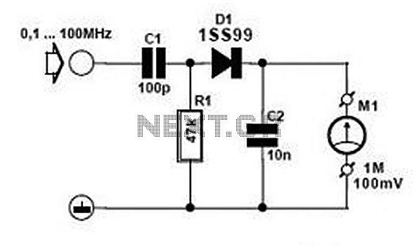
Comprehensive information about RF Probe Circuits is available. Users can learn about and download RF Probe Circuit designs online. RF Probe Circuits are essential tools for testing and analyzing radio frequency signals in various applications, including telecommunications, broadcasting, and electronic...
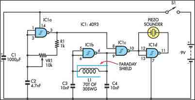
The circuit incorporates two oscillators, both operating at about 40kHz. The first, IC1a, is a standard CMOS oscillator with its frequency adjustable via VR1. The frequency of the second, IC1b, is highly dependent on the inductance of coil L1,...
The circuit depicted in Figure 3-170 illustrates a wound rotor induction motor operating at various speeds, with a voltage (turn difference frequency EMF) U induced in the rotor. The rotor open circuit voltage is represented as Uo (Us0). A...

The adjustment potentiometer for the Raspberry Pi can modify the conduction angle of the thyristor VI and V2, which in turn adjusts the speed of the DC motor M. The speed feedback circuit is implemented using a tachometer generator...
After some minor loss of field magnets, they can be re-magnetized using a homemade method. A scrap of exchanges and contacts, as well as other models like CJ10-60 ~ 15, can be utilized. The circuit operates at 0A (compatible...