
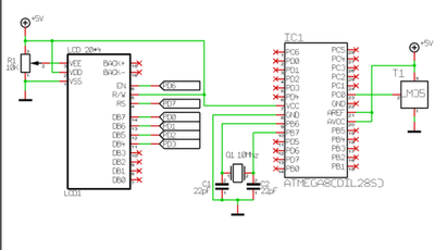
Analog Multiplexer

The AT90S1200A used for the test has a single comparator, but an analog multiplexer was formed using two of its digital bidirectional I/O ports. Notice that for each analog input, there is a 100k resistor, a 0.01 µF capacitor, and a diode. The resistor-capacitor combination forms a low-pass filter, and switching of the charged capacitor is the means by which multiplexing is effected. The technique takes advantage of bidirectional I/O ports to switch from outputs to inputs. In the case of many AVR controllers, the input of the comparator shares a pin with a bidirectional I/O bit. This allows the pin to be held at ground and then ungrounded when using it as an input for the comparator.
Most of the time, the circuit is in the "filtering" state. The inputs are sampled periodically at a low duty cycle as the sampling duty cycle affects cross talk among the inputs. During filtering time, pin 12, which is the input to the comparator, is held at ground and pin 12 (the I/O pin is an output, written with a logic low), Pin 14, which is the multiplexing pin, is open. Under these conditions, the filter capacitor is kept charged to the input voltage (V1).
When it is time for the input voltage to be connected to the comparator input, pin 12 is opened (the I/O pin is made into an input) and the multiplexing pin, pin 14, is connected to +5V (made into an output pin and written with a logic high). This causes the positively charged plate of the capacitor to be connected to +5V through the diode. This results in a Vdd minus one diode drop, minus the voltage on the capacitor being applied to pin 12.
Vpin12 = Vdd - Vdiode - Vin
Where
Vpin12 = the voltage applied to the analog input of the comparator, pin 12,
Vdd = the power supply voltage, 5 volts in this example,
Vdiode = the voltage drop across the diode, which is somewhat dependent on the current through the input resistor, and
Vin = the input voltage applied to the input of the RC filter.
One thing that should be apparent from looking at the expression above is that input voltages are restricted to the range of 0 volts to Vdd-Vdiode, or 0 to about 4.4 volts. As voltages approach 4.4 volts, the current through the diode will become very low, and a noticeable linearity may develop.
The circuit design employs a microcontroller, specifically the AT90S1200A, which is equipped with a single comparator. The use of two digital bidirectional I/O ports allows for the creation of a rudimentary analog multiplexer. Each analog input is connected through a 100kΩ resistor, a 0.01µF capacitor, and a diode, forming a low-pass RC filter. This configuration is crucial for filtering high-frequency noise and stabilizing the input voltage before it is read by the comparator.
The operation begins in a filtering state where the I/O pin (pin 12) is configured as an output, holding it at a low logic level (ground), while the multiplexing pin (pin 14) remains open. This setup keeps the capacitor charged to the input voltage, allowing it to stabilize before sampling. When sampling is required, pin 12 is switched to input mode, allowing the voltage across the capacitor to be read. Simultaneously, the multiplexing pin is set to output a high logic level (+5V), which facilitates the transfer of the stored voltage from the capacitor to the comparator input through the diode.
The mathematical relationship governing the voltage at the comparator input illustrates the limitations of the input voltage range due to the diode's forward voltage drop. This design consideration is essential for ensuring that the analog signal remains within the operational limits of the microcontroller's ADC, preventing saturation or erroneous readings. The overall architecture allows for efficient multiplexing of multiple analog signals while maintaining signal integrity through careful filtering and voltage management.This technique uses digital I/O pins to multiplex analog voltages into an analog input on the microcontroller. The method is most suitable for signals that do not need to be sampled frequently and it may be extended to accommodate a large number of inputs, though for a large number of inputs, the use of a separate analog multiplexer or a mincrocontroller with an integrated multiplexer would often be a better choice.
The AT90S1200A used for the test has a single comparitor, but an analog multiplexer was formed using two of its digital bidirectional I/O ports. Notice that for each analog input, there is a 100k resistor, a .01 uf capacitor, and a diode. The resistor-capacitor combination form a low pass filter and switching of the charged capacitor is the means by which multiplexing is effected.
The technique takes advantage of bidirectional I/O ports to switch from outputs to inputs. In the case of many AVR controllers, the input of the comparitor shares a pin with a bidirectional I/O bit. This allows the pin to be held at ground and then ungrounded when using it as an input for the comparitor.
Most of the time, the circuit is in the "filtering" sate (see the illustrations above). The inputs are sampled periodically at a low duty cycle as the sampling duty cycle affects cross talk among the inputs. This is discussed in more detail below. During filtering time, pin 12, which is the input to the comparitor is held at ground and pin 12 (the I/O pin is an output, written with a logic low), Pin 14, which is the multiplexing pin, is open.
Under these conditions, the filter capacitor is kept charged to the input voltage (V1). When it is time for the input voltage to be connected to the comparitor input, pin 12 is opened (the I/O pin is made into an input) and the multiplexing pin, pin 14, is connected to + 5V (made into an output pin and written with a logic high). This causes the positively charged plate of the capacitor to be connected to +5V through the diode. This results in a a Vdd minus one diode drop, minus the voltage on the capacitor being applied to pin 12.
Vpin12 = Vdd - Vdiode - Vin Where Vpin12 = the voltage applied to the analog input of the comparitor, pin 12, Vdd = the power supply voltage, 5 volts in this example, Vdiode = the voltage drop across the diode, which is somewhat dependent on the current through the input resistor, and Vin = the input voltage applied to the input of the RC filter. One thing that should be apparent from looking at the expression above, is that input voltages are restricted to the range of 0 volts to Vdd-Vdiode, or 0 to about 4.4 volts.
As voltages approach 4.4 volts, the current through the diode will become very low, and a noticeable linearity may develop. 🔗 External reference
Related Circuits
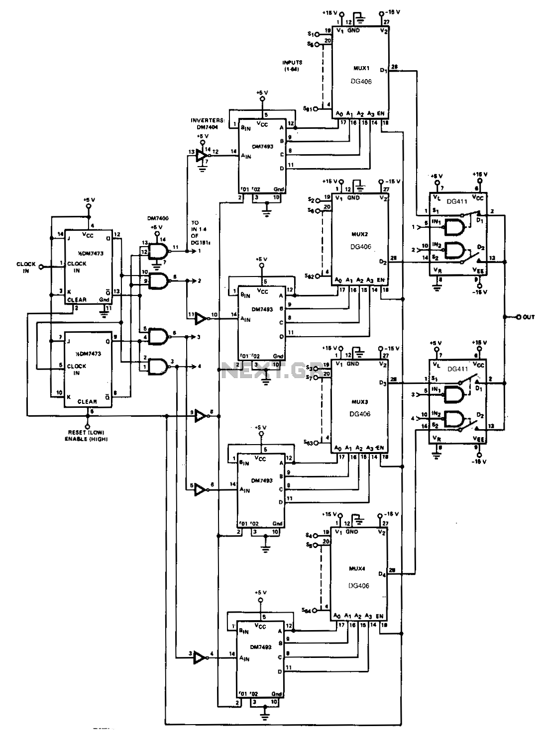
When a large number of channels are multiplexed, the outputs of two or more multiplexers can be connected together, and each multiplexer can be enabled sequentially. In the inhibit mode, the multiplexer consumes less power, and its output and...
The input signal is processed with an electronic low-pass filter to eliminate all frequencies above the Nyquist frequency, which is half of the sampling rate. This process is essential to prevent aliasing during sampling and is referred to as...
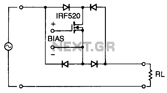
Utilizing four diodes in an array enables the use of a single MOSPOWER transistor for analog switching. The current flow is managed by maintaining the source-base connection of the MOSFET towards the load. It is essential to select diodes...

A video switch is necessary to multiplex several video sources, allowing multiple cameras to be displayed sequentially on a single monitor. This multiplexing process... A video switch serves as a critical component in video signal management, particularly in applications where...
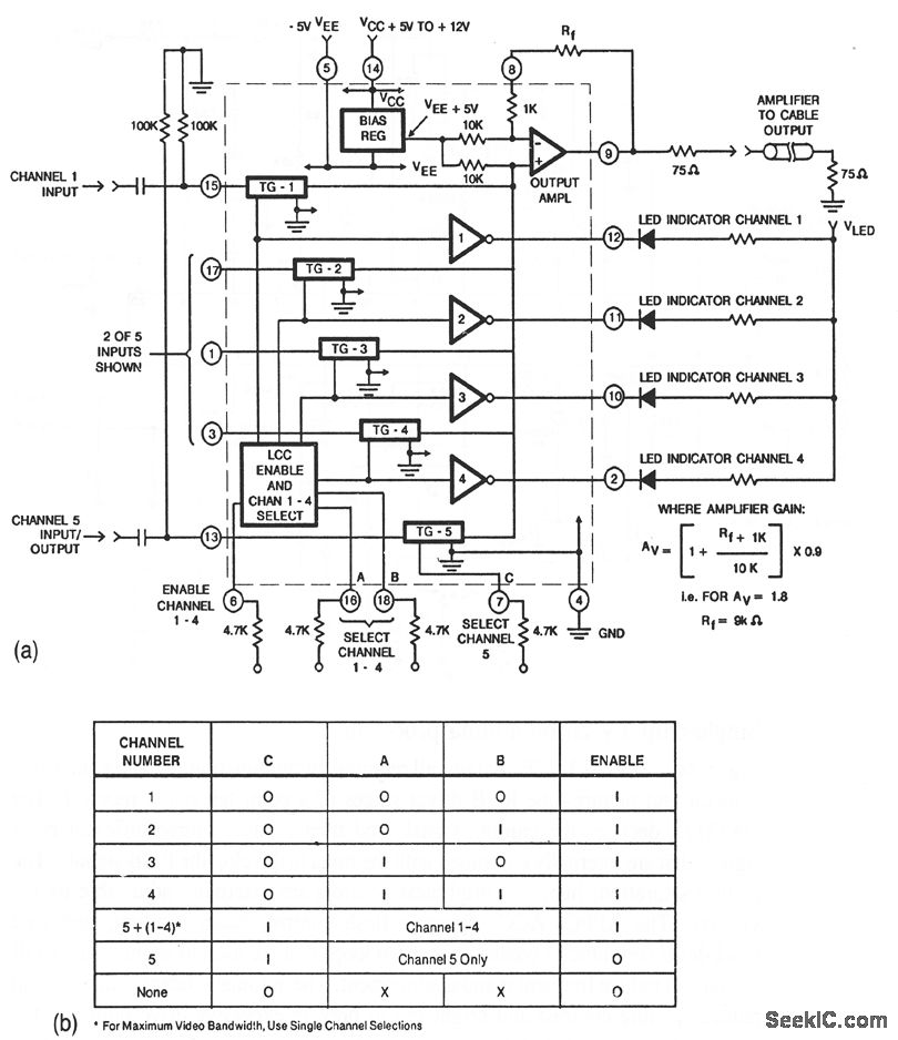
This circuit illustrates a CA3256 switch/amplifier configured for a direct-coupled output. One of four channels can be selected in parallel with channel 5. The analog switches of channels 1 to 4 are digitally controlled by logic. A VEE of...
An Analog-to-Digital Converter (ADC) is a circuit integrated into a single chip designed to convert analog signals into digital signals. Typically, an 8-bit ADC chip converts an analog signal ranging from 0 to 5 volts into a digital level...