
Analog to Digital Converters (AD)
")
The successive approximation analog-to-digital converter (SAR ADC) operates by iteratively narrowing down the value of the analog input voltage through a series of comparisons. The core components include a comparator that evaluates the output of the digital-to-analog converter against the input voltage, a successive approximation register that manages the bit-setting process, and output latches that hold the final digital representation.
During the conversion process, the SAR initiates by resetting itself and setting the most significant bit (MSB). The comparator's role is crucial, as it determines whether to keep or reset each bit based on the outcome of the comparison. The iterative process continues until all bits have been processed, culminating in a digital representation that closely matches the analog input. The conversion complete (CC) signal serves as a flag to indicate that the output data is valid and ready for use.
This architecture allows for efficient and accurate conversion of analog signals into digital form, making it suitable for various applications such as digital signal processing, data acquisition systems, and microcontroller interfacing. The design's ability to produce both parallel and serial outputs enhances its versatility in different electronic systems, facilitating integration with various digital devices and communication protocols.This type of converter is used to convert analog voltage to its corresponding digital output. The function of the analog to digital converter is exactly opposite to that of a DIGITAL TO ANALOG CONVERTER. Like a D/A converter, an A/D converter is also specified as 8, 10, 12 or 16 bit. Though there are many types of A/D converters, we will be discus sing only about the successive approximation type. A successive approximation A/D converter consists of a comparator, a successive approximation register (SAR), output latches, and a D/A converter. The circuit diagram is shown below. The main part of the circuit is the 8-bit SAR, whose output is given to an 8-bit D/A converter. The analog output Va of the D/A converter is then compared to an analog signal Vin by the comparator.
The output of the comparator is a serial data input to the SAR. Till the digital output (8 bits) of the SAR is equivalent to the analog input Vin, the SAR adjusts itself. The 8-bit latch at the end of conversation holds onto the resultant digital data output. At the start of a conversion cycle, the SAR is reset by making the start signal (S) high. The MSB of the SAR (Q7) is set as soon as the first transition from LOW to HIGH is introduced. The output is given to the D/A converter which produces an analog equivalent of the MSB and is compared with the analog input Vin.
According to the comparator output, the SAR will either keep or reset the Q6 bit. This process goes on until all the bits are tried. After Q0 is tried, the SAR makes the conversion complete (CC) signal HIGH to show that the parallel output lines contain valid data. The CC signal in turn enables the latch, and digital data appear at the output of the latch. As the SAR determines each bit, digital data is also available serially. As shown in the figure above, the CC signal is connected to the start conversion input in order to convert the cycle continuously.
Be the first of your friends to get free diy electronics projects, circuits diagrams, hacks, mods, gadgets & gizmo automatically each time we publish. Your email address & privacy are safe with us ! 🔗 External reference
Related Circuits
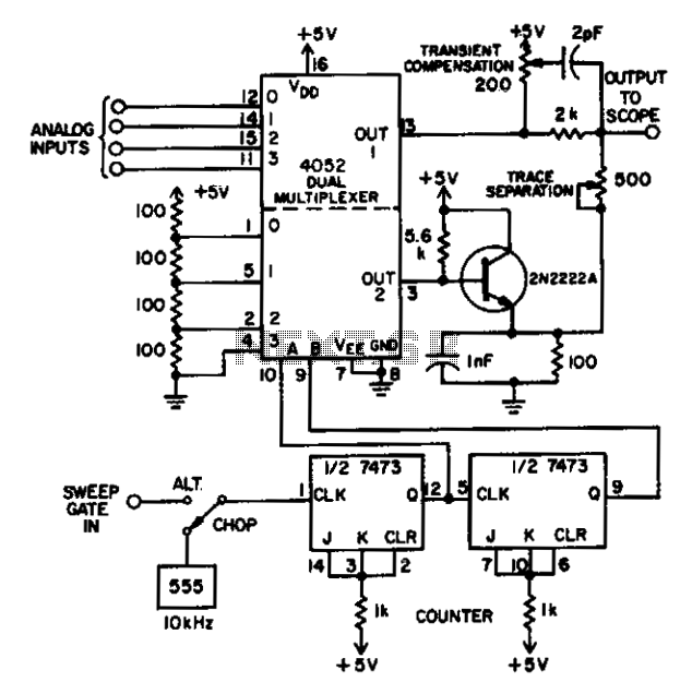
This adapter circuit, which utilizes a dual four-channel analog multiplexer, is capable of handling digital signals up to at least 1 MHz and analog signals throughout the audio range. The upper section of the dual multiplexer is responsible for...
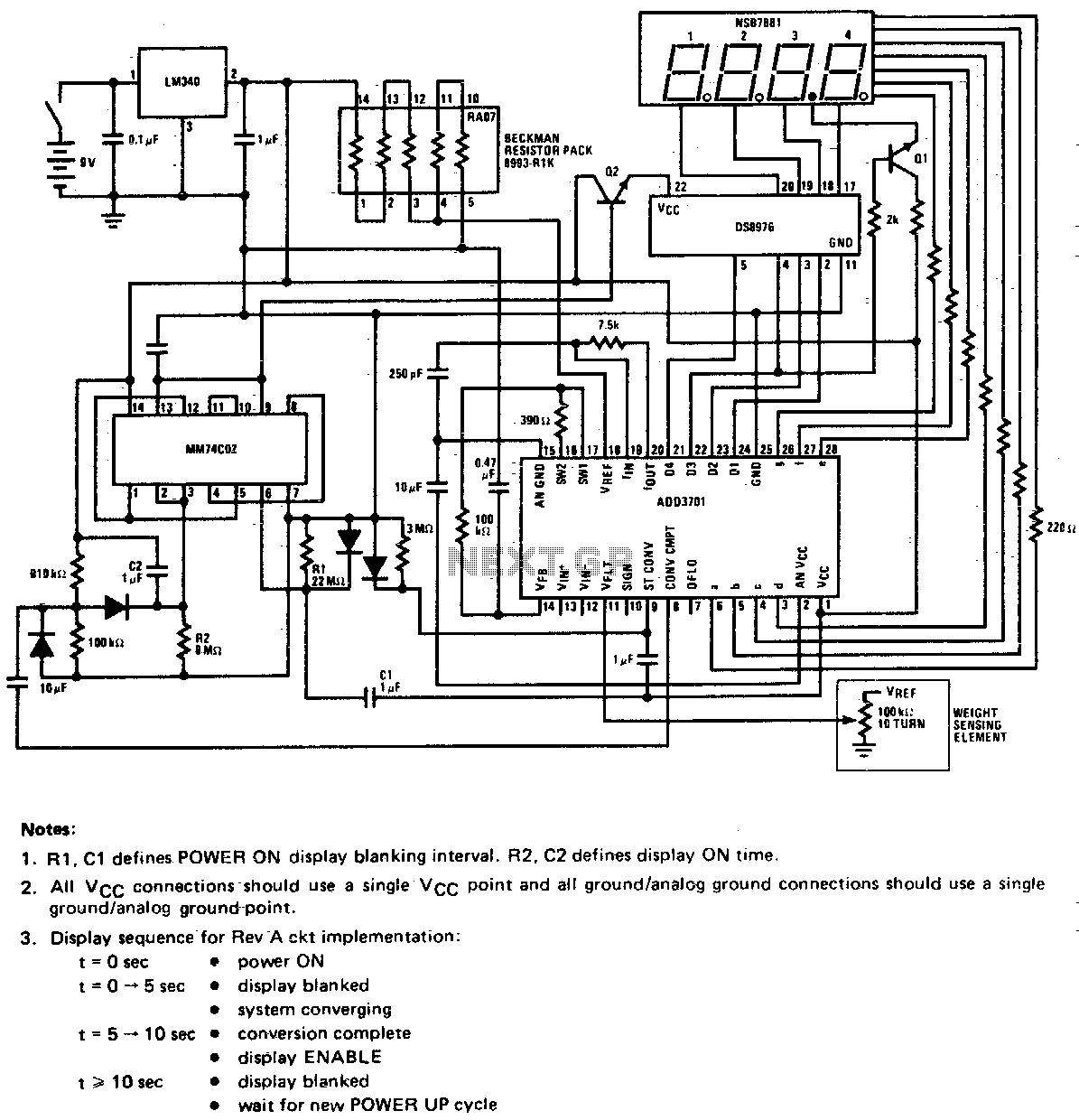
This circuit utilizes a potentiometer as the weight sensing element. An object placed on the scale displaces the potentiometer wiper by an amount proportional to its weight. The conversion of the wiper voltage to digital information is carried out,...
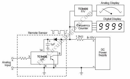
If the sensor system requires an active supply, a single pair of cables can be utilized to transmit both the power supply and the output signal. This approach simplifies the overall system. In sensor systems that necessitate an active power...
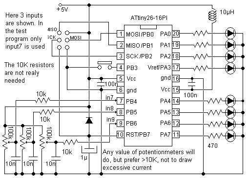
Study the Analog to Digital capabilities of Atmel ATtiny26. This tiny but mighty IC is really a miracle. One special thing is the internal 10-inputs multiplexed ADC circuit which can convert analog voltages to bytes. This check circuit uses...

An analog-to-digital converter (ADC) transforms an analog input voltage into a digital value. This circuit illustrates the operation of an ADC, utilizing the ATmega8 microcontroller to control its functionality. The resolution of the converter denotes the number of discrete...
A Zener diode (D1) is utilized to limit the voltage to the first 6 V of the scale, resulting in a meter reading range of 6 to 8 V, which is beneficial for monitoring automotive electrical systems. The circuit employs...