
And broadening the delay circuit
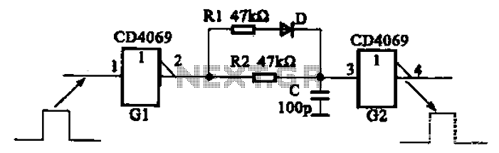
The described circuit utilizes a CD4069 hex inverter to implement a delay and pulse width modulation functionality. The configuration consists of two main stages: the charging and discharging phases of the capacitor C, which are influenced by the resistors R1 and R2.
In the charging phase, when the output of inverter G1 is high, the capacitor C charges through the resistor R1 and the diode D. The diode ensures that current flows in one direction, allowing the capacitor to charge efficiently. The rate at which the capacitor charges is determined by the RC time constant, τ = R1 * C. The voltage across the capacitor rises exponentially until it reaches the threshold voltage of the next inverter stage, G2.
When the output of G1 transitions to a low state, the capacitor C begins to discharge through resistor R2. The discharge rate is governed by the time constant τ = R2 * C. Given that R2 is set to be ten times the value of R1, the discharge time becomes significantly longer than the charging time. This results in a delayed output pulse at G2, which effectively widens the output pulse compared to the input signal.
This configuration is particularly useful in applications where pulse width modulation or timing adjustments are necessary, such as in signal processing, timer circuits, or digital logic applications. The selection of resistor and capacitor values allows for customization of the delay and width of the output pulse, making the circuit versatile for various electronic designs. By inverter Gl, delay and width morning circuit 02 (CD4069) and RC integrating circuit configuration shown. When not gate output high when OI, C capacitor through Rl, D charge, C voltage quickly filled to G2 input threshold level. When Gl output low, C through R2 to the output terminal Gl of low level discharge, due R2-10Rl, therefore, C discharge time is 10 times the charging time. Therefore, the output pulse is delayed while G2 is widened.
Related Circuits

This is a UHF band TV antenna preamplifier circuit with a gain of 15 dB, built using a BF180 UHF transistor. The circuit is straightforward in design. The operational principle consists of two stages. The first stage features a...

This is an improved IR remote control extender circuit. It has high noise immunity, is resistant to ambient and reflected light and has an increased range from remote control to the extender circuit of about 7 meters. It should...

The circuit is depicted. It is capable of both manual and automatic control. The circuit in question is designed to facilitate dual modes of operation: manual and automatic control. This versatility allows users to engage with the system according to...
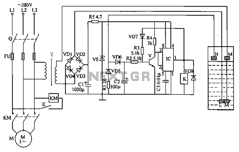
The circuit functions as a liquid level automatic controller, comprising a power circuit, a level detection circuit, and a control execution circuit. The power circuit includes a knife switch (Q), fuse (FU), power transformer (T), rectifier diodes (VD1 to...
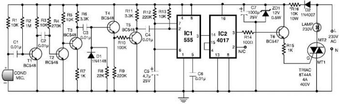
This 555 timer clap switch circuit electronic project is designed using common electronic components. The circuit operates from a distance of up to 10 meters from the microphone. The signal from the microphone is amplified by transistors T1, T2,...
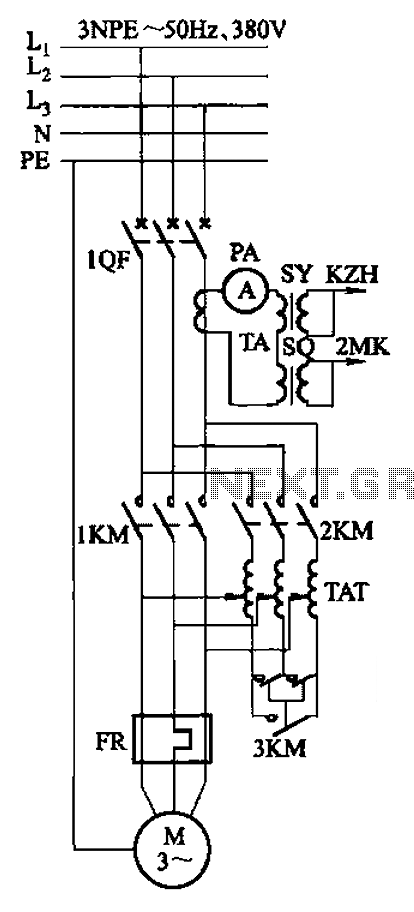
Autotransformer voltage starting, with an adjustable starting time of 30-60 seconds. It includes the SDJ electrode liquid level sensor of HJ-13 type, a pump control system box of HKD-21B type, 1MK level modules adopted by HKG-1SG type, 2MK start...
Warning: include(partials/cookie-banner.php): Failed to open stream: Permission denied in /var/www/html/nextgr/view-circuit.php on line 713
Warning: include(): Failed opening 'partials/cookie-banner.php' for inclusion (include_path='.:/usr/share/php') in /var/www/html/nextgr/view-circuit.php on line 713