
Arduino sampling code and circuit schematic

In the context of electronic circuit design, modularization of code is akin to structuring a circuit into functional blocks or modules. Each module can represent a specific functionality, such as signal processing, data acquisition, or control logic. This approach not only enhances clarity but also facilitates debugging and testing, similar to how functions in programming allow for isolated testing of specific tasks.
In the design of an electronic schematic, attention should be given to how each module interacts with others. For instance, a data acquisition module could gather input from sensors, while a signal processing module could filter and analyze this data, removing noise and outliers to ensure accurate readings. The output from the signal processing could then be fed into a control logic module, which would make decisions based on the processed data, such as activating an actuator or sending data to a user interface.
When designing such a circuit, it is crucial to consider the specifications of each component, including their tolerances and how they handle variations in input. This is similar to the challenges faced in programming when dealing with outliers in data sets. In both cases, robust methods must be employed to ensure reliable performance. For example, in a circuit, using operational amplifiers with high common-mode rejection ratios can help minimize the impact of noise, analogous to statistical methods used in programming to handle outliers effectively.
Overall, a well-structured electronic schematic that reflects the principles of modular programming can lead to improved functionality, easier maintenance, and enhanced performance of the overall system.I started implementing the code I talked about in the last post. Everything is getting a little messy, so I pulled everything out into functions, which made things easier. It`s here, along with all the other code. I had some trouble computing averages while taking out outliers, so I started with just taking a population of.
🔗 External reference
Related Circuits
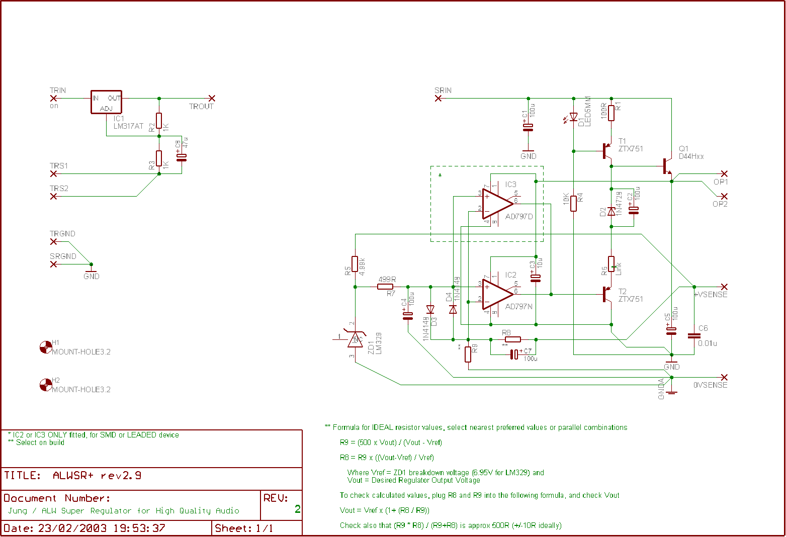
The reference selected is an LM329 sub-surface (or buried) zener (ZD1). While the circuit symbol resembles that of a zener diode, it functions as an active device, resulting in a significantly lower dynamic impedance of approximately 1 ohm compared...
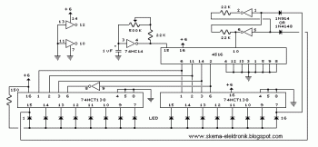
The bi-directional sequencer utilizes a 4-bit binary up/down counter (CD4516) and two "1 of 8 line decoders" (74HC138 or 74HCT138) to create the well-known "Night Rider" display. A Schmitt Trigger oscillator generates the clock signal for the counter, with...
Clearly indicate on the circuit diagram each type and size of the components. There is a need for assistance in designing a low power FM transmitter circuit, specifically using the BA1404 FM transmitter with a center frequency of 79W...
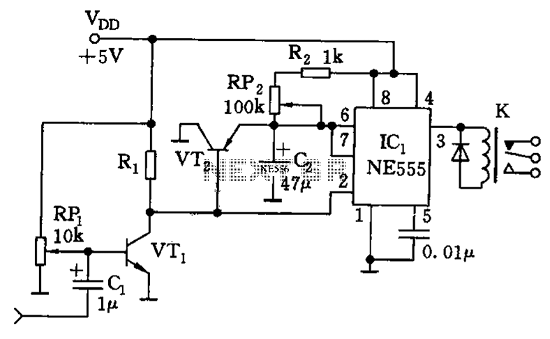
The timing circuit utilizes the 556 dual time base circuit, which includes an intermediate access N8281 crossover network. This design does not require a large volume capacitor, allowing for extended time delays. Initially, the first half of the 556...
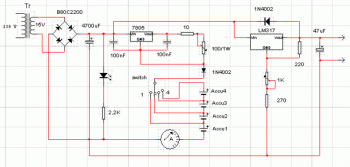
This circuit consists of two main components: a battery charger that provides a fixed output voltage of 5V DC, and a regulated power supply that allows for an adjustable output voltage ranging from 2 to 9 volts. The circuit design...
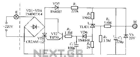
This circuit is a touch-sensitive lamp delay switch characterized by minimal static power consumption. It utilizes an external switch terminal, which can directly replace a standard switch. The circuit features a novel precision voltage regulator integrated circuit, such as...