
jung schematic

The circuit utilizes the LM329 zener diode as a precision voltage reference, taking advantage of its low dynamic impedance to maintain stability in the output voltage. The biasing strategy employed ensures that the voltage reference remains stable and unaffected by noise, enhancing the overall performance of the circuit. The RC filtering network is critical in smoothing out any fluctuations in the reference output, while the selected components are chosen for their optimal performance characteristics. The design also incorporates protective diodes to safeguard the op-amp inputs, reflecting a comprehensive approach to circuit robustness. By employing remote sensing techniques, the circuit improves regulation accuracy, particularly in applications where wiring resistance could otherwise introduce significant errors. The integration of a bypass capacitor further enhances the stability and performance of the error amplifier, ensuring that noise does not adversely affect the output. The power supply arrangement for the error amplifier is particularly innovative, allowing for enhanced PSRR and overall circuit performance. The start-up sequence is meticulously designed to ensure reliable operation from the moment power is applied, highlighting the importance of each component in achieving a stable and efficient voltage regulation system.The reference chosen is an LM329 sub-surface (or buried) zener (ZD1). Whilst the circuit symbol is that of a zener, it`s actually an active device, which results in much lower dynamic impedance than a normal zener, of around 1ohm. It also has low noise relative to it`s output voltage (6. 95V nom. ), due to the sub-surface zener reference. Other devi ces can be used, depending upon desired output voltage / noise performance. This Zener is biased through a resistor (R5). Note though that the bias voltage is from the regulator +ve sense point, or output, which is the quietest +ve rail of the system. Biasing the device in this manner means that the reference is well isolated from the effects of noise at the regulator input, in effect benefiting from a super-reg to itself!
The output of the reference is then filtered, via a simple RC network (R7 / C4). The resistor values are chosen so that the error amplifier (IC2 or IC3) inputs see a low, and matched source impedance of 500 Ohms, thereby facilitating optimum DC stability and dynamic performance and minimising EMC susceptibility. C4 is a very high performance, low E. S. R. device in order to maximise the filtering effect from the low impedances used. The low impedances bring benefits in terms of reducing the inherent noise of the resistors (Johnson noise) and reducing the effects of EMC / EMI on the circuit.
D3 and D4 provide protection against excess differential mode voltage at the op-amp inputs. They are not strictly necessary for the AD797 op-amp, and can be left out for some very minor performance improvement, since the AD797 incorporates these diodes internally. This not the case for many other op-amps though. The reference voltage at the input of the op-amp is compared to a proportion of the output voltage, via the +VSENSE and 0VSENSE inputs and a potential divider (R8 / R9).
+VSENSE / 0VSENSE can be connected directly to the relevant regulator outputs, or to the load (Remote Sensing), thereby improving performance by ensuring the regulator performance is not degraded by the interconnecting wiring`s finite impedance. The ratio of these two resistors sets the output voltage, and the combined parallel impedance of these two values should be 500 Ohms, for optimum dynamic and DC stability.
To prevent noise being amplified by the gain of the error amplifier, the noise gain is reduced to unity at high frequencies, by the addition of a bypass capacitor (C7). This is matched in value and type to C4, in order to equalize AC impedances at the error amp inputs, thereby improving dynamic performance.
The error amplifier also obtains its power from the regulator output (bootstrapping), this brings major performance improvements, and is a fundamental feature of the design. As the error amplifier PSRR (Power Supply Rejection Ratio) degrades, with increasing frequency, the regulator performance will normally suffer.
This connection scheme augments the error amplifier performance dramatically, giving a significant, frequency-dependant, improvement in the regulator performance parameters. In particular line rejection is enhanced significantly. Start-up needs careful consideration though, and is covered in more detail later and helps dictate final topology chosen.
The output of the regulator is from the series pass device (Q1). This is controlled from an LED-biased current source (T1 / R1 / D1 / R4). At switch on the current source provides current to Q1 base, which turns it on causing the output voltage to rise. This applies power to the error amplifier and reference, which then starts to control the output voltage, by sinking current (via T2 / R6 / D2) away from the base, reaching equilibrium when the correct output voltage is achieved.
The level shift Zener diode (D2) is an essential part of the start-up process, ensuring that if the error amp comes on in a low-output condition there is still enough current available at Q1 base 🔗 External reference
Related Circuits

Construct a variable 5A, 2V to 25V regulated power supply using the LM338 adjustable regulator. A power supply schematic and parts list are provided here. The LM338 adjustable voltage regulator is a versatile component capable of providing a regulated output...
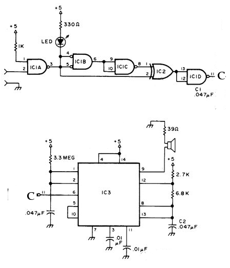
The NE556 timer can function as an indicator for the static state of a digital logic audible terminal. An audible logic probe is beneficial for visually inspecting a component while simultaneously checking the logic state at another point far...
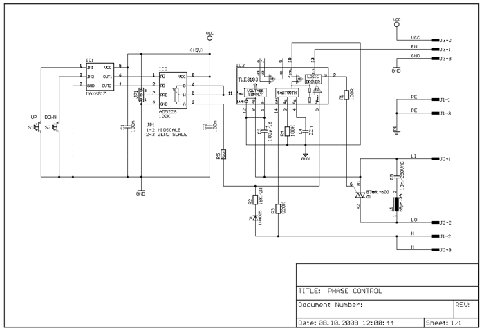
The following circuit illustrates a 2500W Phase Control Circuit Schematic. Features include a ground-tied trigger output that is disabled, and a low voltage input. The 2500W Phase Control Circuit is designed to regulate the power delivered to a load by...
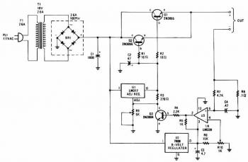
The charger is capable of charging a single cell or multiple series-connected cells with a maximum voltage of 18V. Power transistors Q1 and Q2 are configured as series regulators to manage the output voltage and charging current of the...
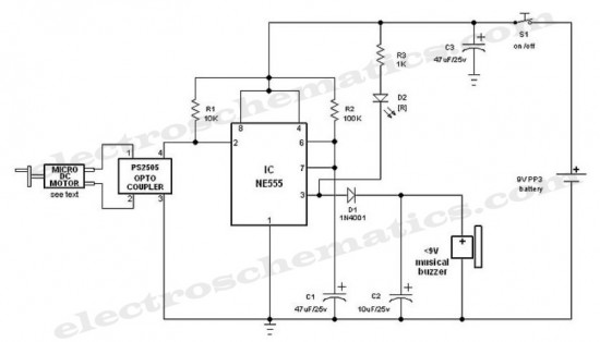
This is an interesting hobby circuit for a crank doorbell. The circuit is built around a 555 timer and a musical piezo buzzer, powered by a 9-volt battery. A single 9-volt PP3/6F22 compact battery is sufficient to power the...
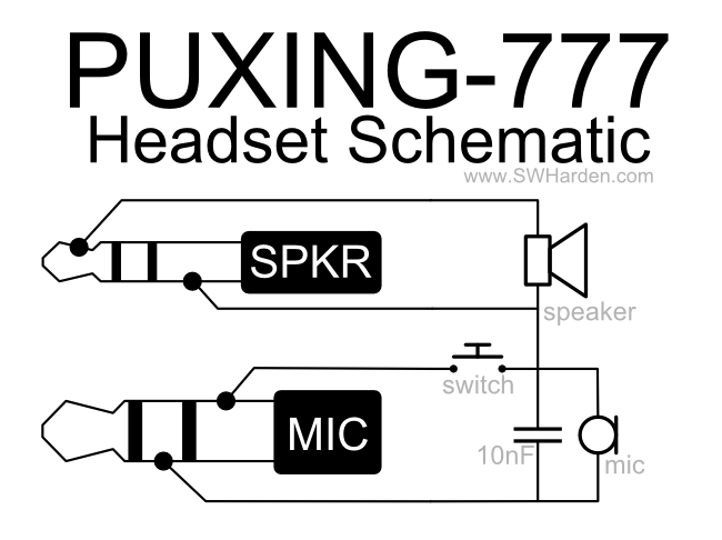
A speaker, microphone, and transmit button circuit designed for the Puxing 777 radio, which is likely compatible with all Puxing radios. The circuit was reverse-engineered from an earphone/microphone headset that originally accompanied the radio to understand its functionality. The...