
Audio Thermostat LM56 ProjectCircuit

The LM56 thermostat circuit utilizes the LM56 integrated circuit, which is designed for temperature control applications. The circuit typically includes a temperature sensor, the LM56 IC, and a set of resistors (R1, R2, R3) that form a voltage divider network. This configuration allows the circuit to monitor the temperature and activate or deactivate a connected load based on predefined temperature thresholds.
In this schematic, the two trip points, VT1 and VT2, are critical for setting the operational limits of the thermostat. The trip point VT1 is set to activate the output when the temperature exceeds a certain threshold, while VT2 serves as a lower limit for deactivation. The equations provided for VT1 and VT2 illustrate how the resistor values influence these thresholds. Adjusting R1, R2, and R3 will therefore modify the voltage levels at which the thermostat responds to temperature changes.
The LM56 features built-in hysteresis, which prevents rapid cycling of the output when the temperature hovers around the set points. This is essential for maintaining stable operation and preventing wear on connected devices. The output can be configured to drive a relay or directly control heating or cooling systems, providing a versatile solution for various temperature regulation needs.
Overall, the LM56 thermostat circuit is a robust design suitable for applications in climate control systems, industrial automation, and other environments where precise temperature management is crucial. Proper selection of the resistor values and understanding of the voltage divider principle are key to optimizing the performance of this thermostat circuit.Thermostat LM56 Project Circuit Diagram LM56 Thermostat Project Circuit Diagram values of R1, R2 and R3 for the required trip points VT1 and VT2 can be determined using the subsequent equations. VT1 = 1.250V x (R1)/ (R1 + R2 + R3) VT2 = 1.2.. 🔗 External reference
Related Circuits
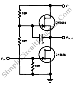
This is a simple high-gain JFET audio amplifier circuit. This circuit requires very low power but provides a high-gain amplification function. It is also referred to as JFET. The JFET (Junction Field Effect Transistor) audio amplifier circuit is designed to...
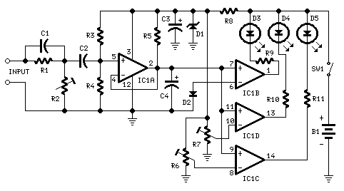
This circuit is designed to indicate the power output level of any audio amplifier. It is simple, portable, and displays three power levels that can be set to any desired value. The circuit operates by utilizing a combination of resistive...
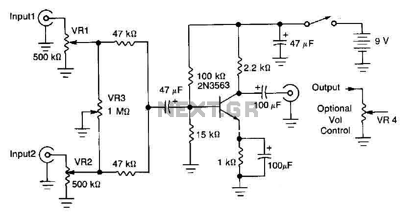
This circuit mixer features internal amplification using a 2N3563 transistor. Two input signals can be independently adjusted via VRI and VR2. The VR3 balance control allows for the attenuation of one signal while the other remains active. Additionally, the...
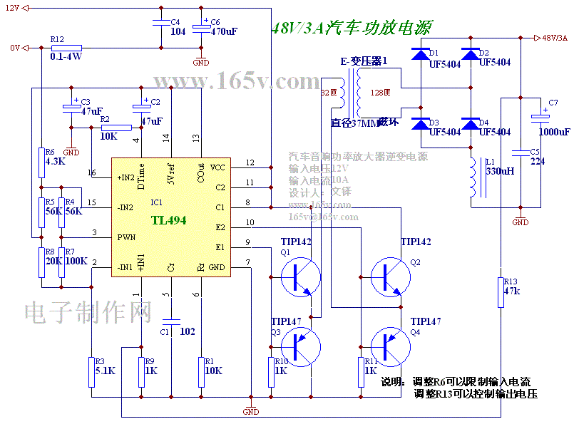
The TL494 controls a car's audio inverter power supply, which is a high-fidelity audio power supply designed for custom vehicles. It operates reliably without the need for adjustments according to the provided circuit diagram. The TL494 is a versatile integrated...
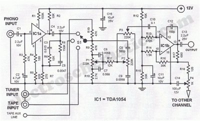
This Hi-Fi stereo preamplifier circuit is constructed using the TDA1054 integrated circuit (IC) from SGS. The TDA1054 is housed in a 16-pin DIL package and incorporates two separate preamplifier circuits. It is characterized by low noise and minimal issues...
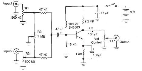
This audio mixer circuit diagram electronic project is designed using a few common electronic components. The audio mixer circuit project has two input channels. The input signal can be independently controlled using the R1 and R2 variable resistors. The...