
Overload speaker protection circuit

The circuit operates as a protective measure for audio amplifiers and loudspeakers, ensuring that excessive power levels do not damage the connected components. The use of capacitors C1 and C2 allows for the detection of potentially harmful signals from both the right and left audio channels. The voltage pulses generated by these capacitors when charged beyond their respective thresholds are crucial for activating the SCR, which serves as a reliable electronic switch.
Relay RY1 plays a pivotal role in this circuit. When triggered by the SCR, it opens the circuit to the loudspeakers, effectively silencing them and preventing any further damage from excessive power. The incorporation of a reset switch (S1) ensures user control over the system, allowing for a manual reset after an over-power condition has been detected.
Calibration is a critical step in the setup process, as it ensures that the circuit responds appropriately to the specific characteristics of the audio amplifier being used. By adjusting the potentiometers R3 and R4, users can fine-tune the sensitivity of the circuit to match the output capabilities of their amplifiers, providing flexibility for different systems. This feature enhances the circuit's usability across a range of audio equipment, making it a versatile solution for speaker protection.
Overall, this circuit design exemplifies a practical approach to safeguarding audio equipment, combining simple yet effective components to create a reliable protective mechanism against over-power conditions.The circuit input is taken from the terminal loudspeaker or amplifier output jacks. If the right channel is large enough to charge C1 to a potential which exceeds the breakdown voltage of the emitter of Ql, a voltage pulse appears in R7. Similarly, if the left channel signal is large enough to charge C2 to a voltage that is greater than the breakdown voltage of the emitter of Q2 ", a pulse appears in R7.
The pulse triggers in R7 5CRI. A door sensitive SCR (LGT less than 15 RNA or IGT is the gate-trigger current) that locks in a conducting state and energizes Ryl. The action of the relay will interrupt the speaker circuit. and silence follows you must alert on the problem. Reduce the volume on your amplifier, then press and release 51 to reset the circuit and restore normal operation. The circuit can be set to go off at any level of 15 watts RMS to 150. To calibrate . deliberately over-power signal at the entrance of the right speaker protection and adjust R3 until RY1 boosts.
Do the same with the left channel, this time adjusting R4. The circuit is now calibrated and ready employment.
Related Circuits
This circuit functions as an RF power amplifier designed to operate with a power supply capable of delivering 13 volts at a current of 10 amperes. Careful assembly of the power source is essential. It utilizes a shielded transformer...

This circuit allows for the observation of movement between various stroboscopes. The generation of a rectangular signal is accomplished using an NE555 timer. It operates on a low power supply, which is created using a simple transformer (TR1), a...

A straightforward smoke detector circuit has been presented through a schematic diagram, which can be easily constructed and installed in an area for essential detection purposes. The circuit utilizes the versatile FIGARO TGS 813 gas sensor as the primary...

This fire sensor circuit utilizes the temperature-sensing capability of a standard signal diode, specifically the IN 34, to detect heat from a fire. Upon detecting heat, it triggers a loud alarm that mimics the sound of a fire brigade....
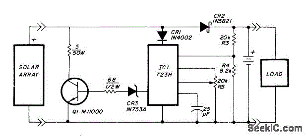
A voltage regulator is connected across the solar cell to prevent damage to the storage battery due to overcharging. A series diode prevents the array from discharging the battery during hours of darkness. The regulator does not draw power...
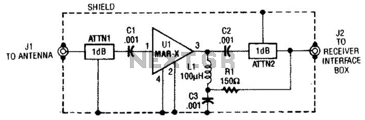
The MAR-x preamplifier is designed to operate within a frequency range of up to 1.5 or 2 GHz, depending on the selected MAR-x integrated circuit (IC). For applications requiring a low noise figure, ATTN1 should be omitted. Both ATTN1...