
Vhf-Uhf Preamp Circuit

The MAR-x preamplifier circuit is an essential component in high-frequency applications, particularly in communication systems where signal integrity is paramount. The choice of the MAR-x IC dictates the operational frequency range, with options available to maximize performance at either 1.5 GHz or 2 GHz.
In configurations where low noise performance is critical, the removal of ATTN1 is recommended. This adjustment minimizes additional noise contributions that can arise from attenuation stages, thus enhancing the overall noise figure of the preamplifier.
ATTN1 and ATTN2 are designed to offer flexibility in signal attenuation, allowing for precise control over the input signal levels. By limiting the termination range, these components help stabilize the circuit, preventing oscillations and ensuring reliable operation under various conditions. The careful selection and implementation of these attenuation stages are crucial in maintaining device stability, particularly in sensitive applications where signal fidelity is essential.
Overall, the MAR-x preamp circuit exemplifies the balance between performance and stability in high-frequency electronic designs, making it a valuable asset in modern RF and microwave engineering. The MAR-x preamp shown will cover up to 1.5 or 2 GHz with the correct MAR-x IC. ATTN1 should be omitted for low noise-figure.appli cations. ATTN1 and ATTN2 provide a means of limiting possible termination range, for less chance of device instability.
Related Circuits
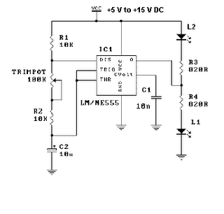
This is a simple LED flasher project that utilizes a common 555 timer integrated circuit (IC) for its operation. It is configured in astable mode, which means its output functions as a square wave oscillator. Two LEDs are connected...
For example, I do not understand the process of demodulation or the modulation itself, and so on. Is there someone who can understand this circuit? Could you please assist me? The circuit in question likely involves a modulation and demodulation...
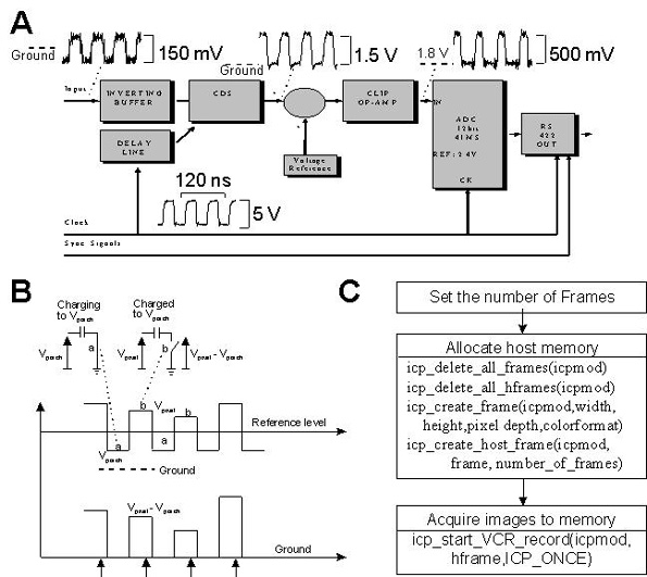
This document provides technical details regarding the hardware and software of a complete imaging system that utilizes a fast CCD sensor and a 41 Msample/s A/D converter. This system is capable of acquiring full-frame digitized images at a resolution...

A simple musical light chaser circuit diagram and schematic using IC CD4016. This circuit blinks lights in response to sound, audio, or music output, causing 10 lights to dance according to sound frequency. The musical light chaser circuit utilizing the...
A circuit designed to operate within a frequency range with an accuracy greater than 2% for generating Bode plots. It converts two sine waves into a square wave, taking into account the overlap relative to the total input wave...

This is a UHF band TV antenna preamplifier circuit with a gain of 15 dB, built using a BF180 UHF transistor. The circuit is straightforward in design. The operational principle consists of two stages. The first stage features a...