
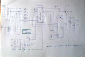
Automatic conversion l0 wind speed controller C192 555 CD4028

The automatic conversion circuit for wind speed control is designed to effectively manage the operation of a motor based on varying wind speeds. The clock signal generator, implemented with a 555 timer IC, is crucial for producing a stable square wave output, which serves as the timing reference for the entire system. The resistors and capacitors associated with the multivibrator allow for precise control over the frequency and duty cycle of the output signal, enabling customization based on specific application requirements.
The counter IC2 (C192) operates in conjunction with the clock pulses from IC1 to count the frequency of the incoming signals. This counting mechanism is essential for translating the frequency of the wind speed into a corresponding binary code. The binary output from IC2 is then decoded by IC3 (CD4028), which transforms the binary-coded decimal (BCD) into a format that can be utilized for controlling the SCR.
The synchronous phase shifting circuit plays a pivotal role in determining the conduction angle of the SCR. By adjusting the output signals of the decoder, the circuit dynamically alters the SCR's firing angle, which in turn influences the power delivered to the motor. This allows for smooth and gradual changes in motor speed, accommodating fluctuations in wind speed effectively. The buck rectifier circuit ensures that the voltage supplied to the control system remains stable, providing the necessary power for reliable operation.
Overall, this circuit exemplifies a sophisticated approach to wind speed control, utilizing a combination of digital and analog components to achieve precise motor control in response to environmental conditions. The design not only enhances operational efficiency but also contributes to the longevity and reliability of the motor system. As shown in Figure 10 for the automatic conversion of wind speed control circuit. The circuit includes a clock signal generator IC1, counter IC2, decoder IC3, synchronous phase shifting circuit (BG1, BG2, BG3), SCR control circuit SCR, buck rectifier circuit. Where the buck rectified voltage stability in (9 ~ 10.5) V, provides power for the entire controller.A clock signal generator is multivibrator IC1 (555), R2, R3, W1, W2, C3 and other components, depending on the frequency of the signal charge and discharge time constant, and can be changed by adjusting the signal W1, W2 of frequency and duty cycle. Low frequency square wave generated by IC1 IC2 as counting pulses and added to the CP side (14 feet).
Corresponding decimal synchronous counter IC2 (C192) generated by A, B, C, D 4-bit binary code is added to decimal decoder IC3 (CD4028), with the addition of CP, which translated BCD code at the output Q0, Q1. Q8, Q9 turn was high, so is the wind speed change gear provides the basis for automatic conversion.Synchronous phase shifting circuit sequentially enables IC3 output signal change, thus changing the thyristor SCR conduction angle, the motor terminal voltage changes in turn, automatically converting 10 wind speed.
Related Circuits
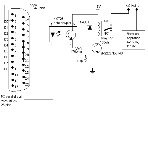
Here is a circuit for using the printer port of a PC for control application using software and some interface hardware. The interface circuit along with the given software can be used with the printer port of any PC...
This is the circuit diagram of a touch-activated alarm system that remains operational during power outages. The alarm system is triggered when someone touches the designated touch plate. A notable feature of this circuit is the automatic battery activator,...

Closing switch S allows the power supply's positive half cycle to flow through VD1, R1, and VD2 to charge capacitor C. The voltage across capacitor C gradually increases but remains significantly lower than the threshold voltage of the zener...
Using a switch to power up your microcontroller projects may not be a good idea if you need to "wake" the PIC during some events. For example: A metal detector sends a pulse indicating a car is ready to...
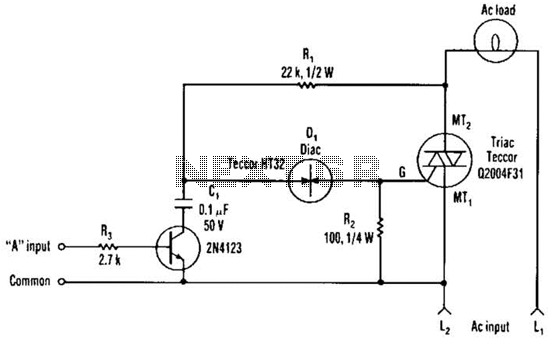
The single transistor connected between the capacitor and the common side of the AC line allows a logic-level signal to control this TRIAC power circuit. Resistor R2 prevents false triggering of the TRIAC by the trickle current through the...
This resource contains step-by-step information for creating an AVR microcontroller programmer, complete with a suitable circuit diagram. This programmer is capable of programming 8051, AT89XX, AT90XXXX, and 8031 family microcontrollers. The AVR microcontroller programmer described is designed to facilitate the...