
Automatic Gain Control Pre-Amplifier

The described circuit utilizes operational amplifiers (op-amps) in conjunction with 1N4148 diodes to create a feedback mechanism that stabilizes the output voltage. The rectification process performed by the diodes converts the AC component of the op-amp's output into a DC signal, which is then smoothed by a filtering stage. This filtered signal is crucial as it controls the gate of a Field Effect Transistor (FET), which acts as a variable resistor in the input path.
The FET input shunting circuit is designed to dynamically adjust the amount of input signal that is allowed to pass through to the output. As the output voltage from the op-amp increases, the control voltage at the gate of the FET also increases, leading to a greater shunting effect. This effectively reduces the amplitude of the input signal that reaches the op-amp, thereby regulating the output voltage to a desired level.
The flexibility of the circuit is highlighted by its ability to set the output level across a range from less than unity gain up to almost the full gain of the amplifier. This feature enables the circuit to be applied in various contexts, such as in automatic gain control systems, signal conditioning applications, or other scenarios where maintaining a stable output level is critical. The integration of the op-amp with the FET shunting mechanism provides a robust solution for managing signal levels in electronic systems.A portion of the op amp`s output signal is rectified by the 1N4148 diodes, then filtered and fed to the gate of the FET input shunting circuit. As the output rises, more and more input shunting takes place. That is, more of the input signal is bypassed, effectively keeping the output level constant. The output output level itself can be set from l ess than unity all the way up to nearly the gain of the amplifier, making the circuit usable in other applications as well. 🔗 External reference
Related Circuits
This circuit is a stable frequency counter with an accuracy of 5 significant digits. It operates within a frequency range of 0 to 30 MHz and has an input sensitivity greater than 100 mV. The probe connects to the...
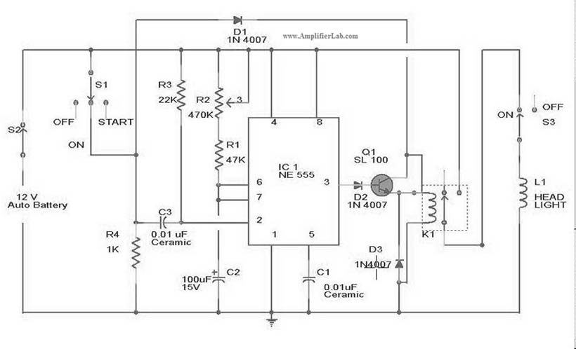
The circuit diagram for the automatic headlights turn-off circuit is presented here. This circuit can be installed in a car. The automatic headlights turn-off circuit is designed to enhance vehicle safety and convenience by ensuring that the headlights are automatically...
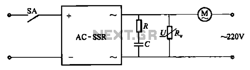
The circuit illustrated in Figure 3-13 is an RC surge absorption circuit that includes a resistor (R) and zinc oxide varistors (such as MY31, MYH12, MYH20 types, etc.), which serve as an overvoltage protection device. The resistance R is...
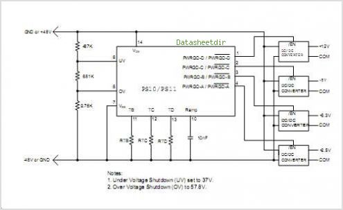
The PS10 saves board space, improves accuracy, eliminates optocouplers or level shifts, and reduces overall component count by combining four programmable timers, input under-voltage (UV) and over-voltage (OV) supervisors, a programmable power-on reset (POR), and four 90V open drain...
This project represents an older design that has likely been replaced by a newer version. Nevertheless, it remains a functional design and can be beneficial for homebrew synthesizer enthusiasts. It should be noted that the majority of these designs...

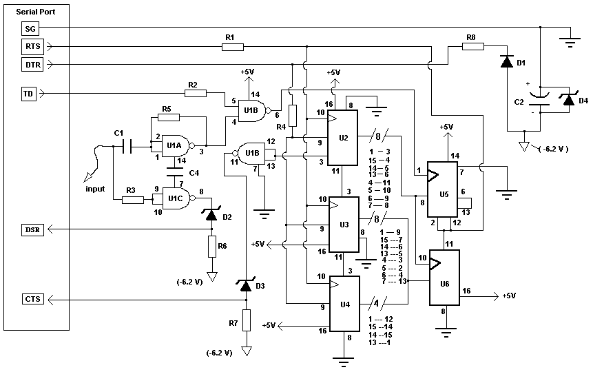
The HC-06 module is a slave mode serial Bluetooth data link manufactured by CSR. In this project, a mobile phone communicates with the AT89C2051 microcontroller via the HC-06 module. The complexity of the communication has been encapsulated within a...