
Three-phase stepper motor control circuit

The described circuit utilizes a DC Solid State Relay (SSR) as an opto-isolator to enhance signal isolation and control capabilities within the system. The LED within the opto-isolator is activated when the switch output is high, generating a corresponding low signal in the driver circuit. This inversion is critical for ensuring that the control logic remains robust against noise and interference.
The photosensitive transistor, once activated by the light emitted from the LED, allows current to flow from the collector, thus producing an output voltage. This output can be interfaced with various external circuits, enabling control over devices such as motors, lights, or other electronic systems. The SSR's output stage is designed to handle voltages between 30V and 180V, making it suitable for a variety of applications that require high voltage management and switching capabilities.
In the context of a three-phase motor system, the SSRs are employed in each phase (A, B, and C) to regulate the current flowing through the motor windings. Each SSR operates in conjunction with the 8255 programmable peripheral interface, which allows for precise control over the phases through ports PA0 to PA2. This configuration enables the system to effectively manage phase timing and power delivery, optimizing motor performance and efficiency. The overall design emphasizes reliability and responsiveness, making it ideal for industrial applications where precise control over three-phase motors is essential.As it can be seen from the figure, + DC Solid State Relay (SSR) of the input stage is an opto-isolator, when the switch output is high, by inverting driver circuit goes low, so there is a light emitting diode and the current through the light, the light of the photosensitive transistor is turned on, so that the collector generates an output voltage which can be used to control external circuitry. SSR power transistors for the output stage, the output voltage of up to 30 -180V. Step into the motor A, B, C three-phase, each phase consists of - a type SSR Yin flow control, respectively, by 8255 the port PAO ~ PA2 controlled.
Related Circuits

This is a reverse-engineered circuit diagram of a one-transistor circuit commonly used to drive permanent magnet DC motors in children's toys. This circuit typically employs the 625mW version of the widely used 8050 or 8550 transistor. It is important...
All resistors have a tolerance of 5 or 10 percent and are rated for 1/4 watt. All capacitors have a tolerance of 10 percent and are rated for 35 volts or higher. This circuit effectively amplifies the output of...
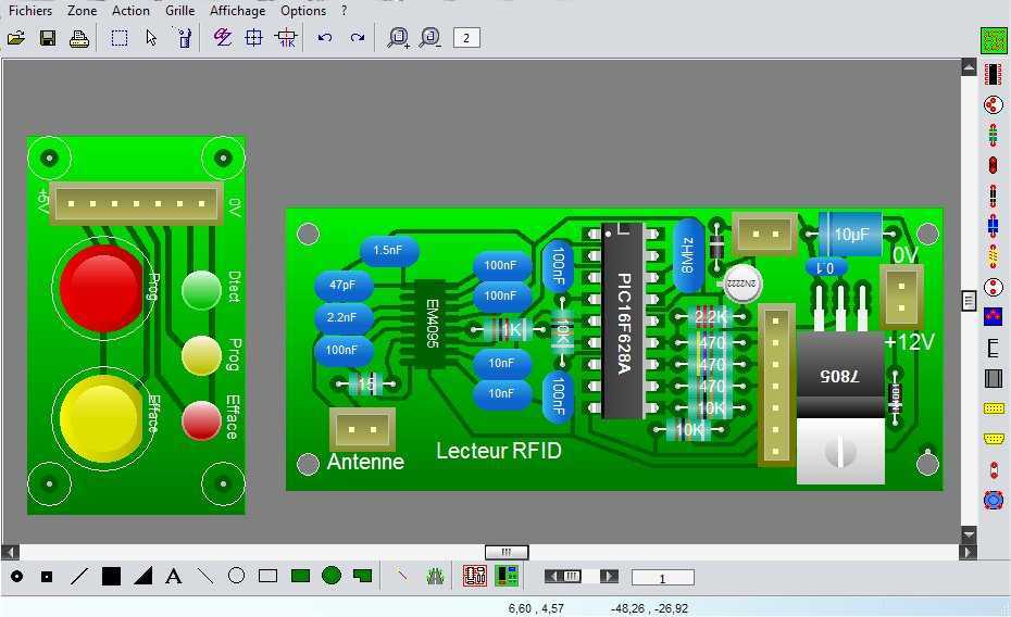
WinCircuit is a software of realization of drawing of printed circuit in single or double layers. Principal qualities are the facility of use and the sight in pseudo 3D which gets a vision of the circuit close to reality....
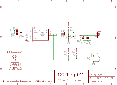
Connect any I2C client chip (such as temperature sensors, analog-to-digital converters, displays, or relay drivers) to your PC via USB quickly, easily, and affordably. Drivers are available for both Linux and Windows operating systems. The described system facilitates the integration...
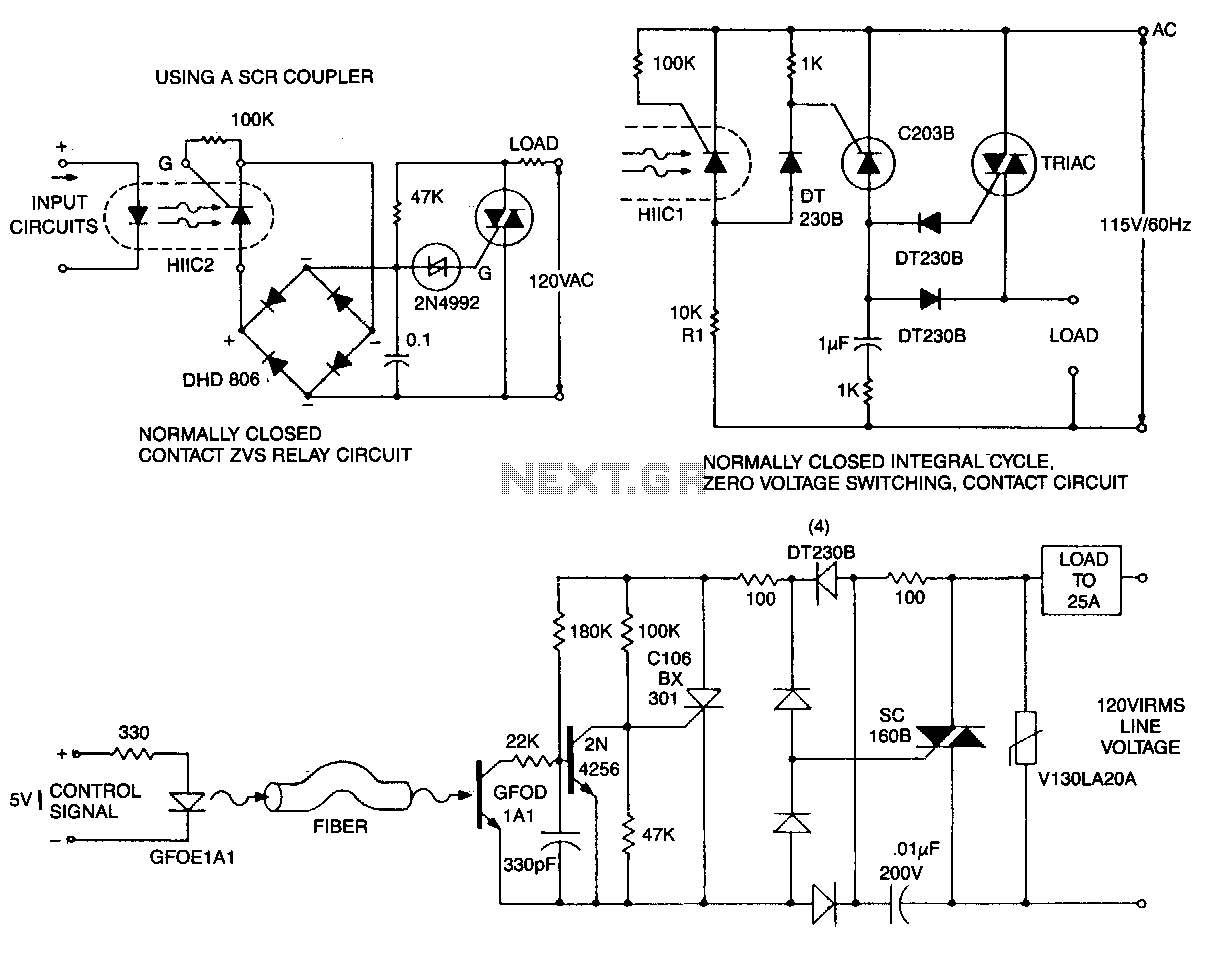
This circuit is effective for lamp and heater loads. Some circuits driving reactive loads require integral cycling and zero-voltage switching when an identical number of positive and negative half-cycles of voltage are applied to the load during a power...
The circuit diagram above illustrates the Clock Controller V1.1. Pins P3.0 to P3.3 are connected to the base of a 4-PNP transistor, specifically the 2N2907, which is used to sink current. The Clock Controller V1.1 circuit is designed to manage...