
Basic FET Amplifier

The FET amplifier circuit operates on the principles of field-effect transistor action, where the gate voltage controls the current flowing from the drain to the source. The circuit typically consists of a single FET transistor, resistors for biasing, and coupling capacitors to ensure that AC signals can pass while blocking DC components.
In this configuration, the source resistor plays a critical role in establishing the operating point of the amplifier. By selecting an appropriate value for the source resistor, the circuit designer can set the desired biasing conditions, ensuring that the FET operates within its linear region for optimal signal amplification. The drain resistor, on the other hand, is essential for defining the output voltage swing and the gain of the amplifier.
The input signal is applied to the gate terminal, where it modulates the gate-source voltage (Vgs). A more positive gate voltage relative to the source increases the channel conductivity, allowing more drain current to flow. Conversely, a less positive gate voltage reduces the drain current, demonstrating the transconductance property of the FET.
The output is typically taken from the drain terminal, where the amplified version of the input signal can be observed. The relationship between the input and output voltages is characterized by the gain of the amplifier, which can be adjusted by varying the values of the resistors in the circuit.
In summary, the FET amplifier circuit is a versatile and efficient design for signal amplification, leveraging the unique characteristics of FET transistors to achieve high input impedance and low output impedance, making it suitable for various applications in electronics.This is The Fet Amplifier circuit. This circuit uses FET transistor. The gate of the FET must be negative with respect to the source, so a bias can be achieved in the following manner. The voltage that is across the source resistor is developed by the drain current flowing through the source resistor.
Due to that action, the emitter become positiv e with respect the zero volts rail. Here is the schematic diagram of the circuit: The fet is biased correctly, since the current does not flow at gate make the gate has a zero volts. So, the gate is negative with respect to the source because the source is positive with respect to the gate.
The drain current is controlled by the signal voltage that is applied to the gate. The drain current will be decreased when the signal goes less positive. It will make the drain voltage goes more positive because just a little voltage across the drain resistor. The drain voltage will goes more negative and more voltage across the drain resistor when the drain current is increased because the signal voltage goes more positive.
So, the drain voltage does the opposite of the gate voltage. We aim to transmit more information by carrying articles. Please send us an E-mail to wanghuali@hqew. net within 15 days if we are involved in the problems of article content, copyright or other problems. We will delete it soon. 🔗 External reference
Related Circuits
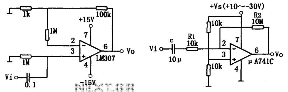
The simple audio amplifier circuit is illustrated in the figure. Utilizing an integrated op-amp configuration, this audio amplifier is stable and allows for easy negative feedback, facilitating the achievement of equalization characteristics. Additionally, the crosstalk between channels is minimal,...
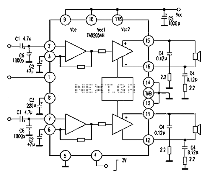
A Mitsubishi Pajero car audio system is experiencing a silent fault, while other features remain operational. The issue is traced to a damaged amplifier IC, specifically the TA8205AH. This integrated circuit, produced by Toshiba, is a dual-channel audio power...
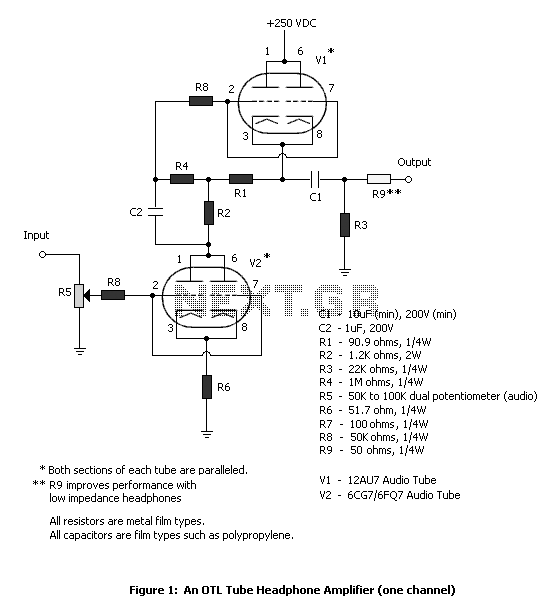
The tube headphone amplifier in figure 1 is a high current mu follower, with a 12AU7 cathode follower driven by a 6CG7. Both sections of each tube are paralleled to minimize noise. It's a zero global feedback, OTL design...
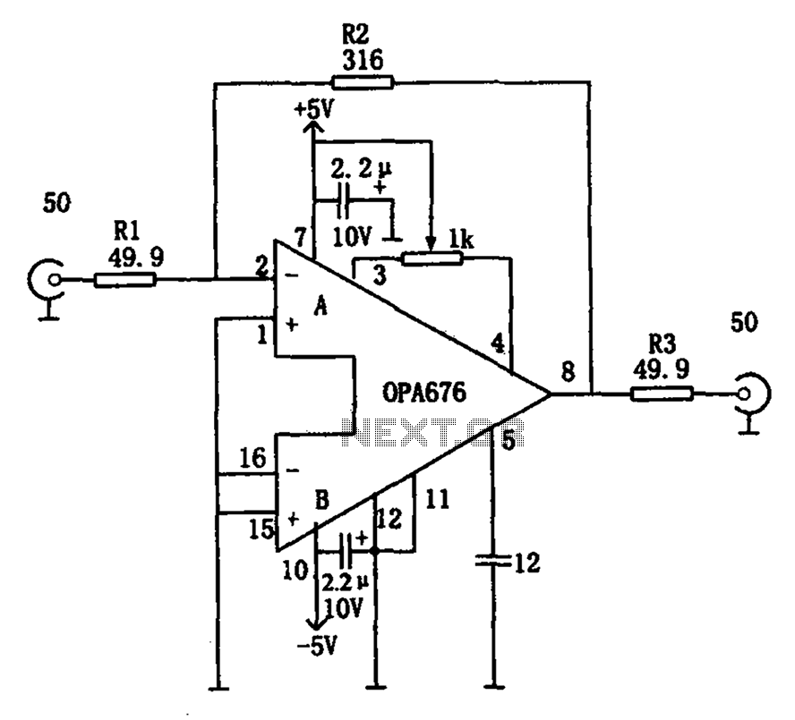
The circuit features a broadband video amplifier with a 50-ohm input/output impedance. To ensure optimal signal transmission and minimize reflected signals, it is often necessary to match the input and output impedances of the amplifier. The broadband video amplifier...
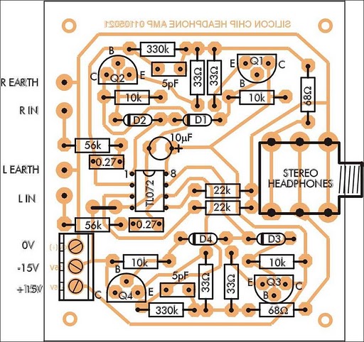
In addition to its primary function as a headphone amplifier, this circuit can be utilized for various applications requiring a wide bandwidth low-power amplifier. It is designed around an operational amplifier (op-amp), with its output current enhanced by a...
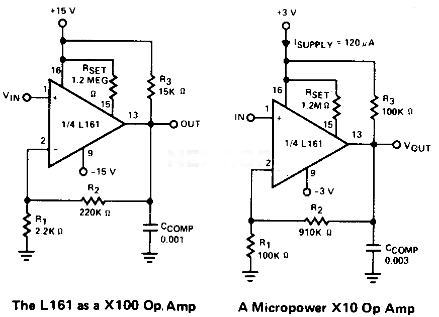
This is a single gain-of-100 amplifier with a gain-bandwidth product of 20 MHz. The primary limitation in performance is the low slew rate of 0.3 V/μs imposed by the charging of Ccomp. The effects of slew rate and compensation...