
Beat Frequency Oscillator

The squelch diode (CR1) connects the output of the first audio frequency (AF) stage to the input of the second. The control transistor (Q1) regulates the circuit. The anode and cathode voltages of CR1 are typically biased positive relative to ground. When no input signal is detected, resistor R9 is adjusted so that Q1 draws sufficient collector current to lower its collector voltage and the anode voltage of CR1 below the voltage at its cathode. Consequently, the anode voltage of the squelch diode becomes negative relative to its cathode, halting conduction and reducing audio output to zero, resulting in a silent receiver. The base of Q1 is linked to the automatic volume control (AVC) line. When a signal enters the receiver, a negative AVC voltage is applied to the base of Q1, decreasing collector current and increasing collector voltage. This, in turn, raises the anode voltage of CR1 until it becomes positive relative to the cathode, allowing diode CR1 to conduct and pass the signal to the second AF amplifier. Thus, diode CR1 operates effectively as a switch controlled by the AVC voltage.
The overall functionality of the BFO and squelch circuit ensures that the receiver can effectively demodulate CW signals while minimizing unwanted noise, thereby enhancing the listening experience. The integration of these components is crucial for achieving optimal performance in communication systems that rely on CW transmission.The beat frequency oscillator (bfo) is necessary when you want to receive cw signals. Cw signals are not modulated with an audio component, you remember, so we must provide one. The action of the rf amplifier, mixer, local oscillator, and IF amplifier is the same for both cw and AM; but the cw signal reaches the detector as a single frequency sign al with no sideband components. To produce an af output, you must heterodyne (beat) any cw signal with an rf signal of the proper frequency. This separate signal is obtained from an oscillator known as a beat frequency oscillator. The picture below is a block diagram of a superheterodyne receiver capable of receiving and demodulating a cw signal.
The bfo heterodynes at the detector and produces an af output. The detector (second detector) is used primarily because the mixer (first detector) is normally used as the source of agc. If the intermediate frequency is 455 kilohertz and the beat frequency oscillator is tuned to 456 kilohertz or 454 kilohertz, the difference frequency of 1 kilohertz is heard in the output.
Generally, you will tune the bfo from the front panel of a receiver. When you vary the bfo control, you are varying the output frequency of the bfo and will hear changes in the tone of the output audio signal. The sensitivity of a receiver is maximum when no signal is being received. This condition occurs, for example, when a receiver is being tuned between stations. At this time background noise is picked up by the antenna, and you will hear noise greatly amplified.
This noise is highly annoying and occurs because receiver gain is maximum without a signal. You can often overcome this problem by using a circuit called a SQUELCH, NOISE SILENCER, NOISE SUPPRESSOR, or NOISE LIMITER. All of these noise type circuits just clip the peaks of the noise spikes. Squelch will actually eliminate noise. The picture below is a typical circuit of this type. The circuit cuts off receiver output when no input signal is being received. It accomplishes this by blocking either the detector or audio amplifier when no signal is present. Let`s take a look at the theory involved in this process. The squelch diode CR1 connects the output of the first af stage to the input of the second. Amplifier Q1 serves as the control transistor for the circuit. The anode and cathode voltages of CR1 are normally biased positive with respect to ground. With no input signal, R9 is adjusted until Q1 draws enough collector current to reduce its collector voltage and the anode voltage of CR1 to a value below the voltage on the cathode of CR1.
At this point the anode voltage of the squelch diode is negative with respect to its cathode, and conduction ceases. Audio output is now reduced to zero and the receiver is silent. The base of Q1 is connected to the automatic volume control (avc) line. Anytime a signal enters the receiver, a negative avc voltage is applied to the base of Q1. This reduces the collector current and increases the collector voltage, which in turn increases the anode voltage of CR1 until the anode becomes positive with respect to the cathode.
Once again diode CR1 will conduct, and the signal will be passed to the second af amplifier. Diode CR1 is effectively a switch controlled by the avc voltage. 🔗 External reference
Related Circuits
The ADF4107 Frequency Synthesizer can be used to implement local oscillators in the upconversion and downconversion sections of wireless receivers and transmitters. It consists of a low noise digital phase frequency detector (PFD), a precision charge pump, a programmable...

An oscillator is an electronic circuit that converts energy from a direct-current source into a periodically varying electric output. An oscillator is a fundamental component in various electronic systems, serving the purpose of generating oscillating signals, typically in the form...
A high-frequency waveform generator is highly beneficial for electronic experimentation and design. This circuit generates sine wave oscillations; however, it can be modified to produce triangle or square wave functions. The frequency can be controlled using current. By disconnecting...
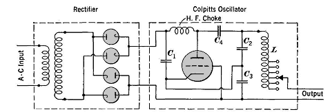
High frequencies are defined as those above 50,000 cycles per second. For industrial power supplies, the Golpitts circuit or the coupled-grid self-excited oscillator circuit is most commonly used. In either circuit, the alternating supply voltage is stepped up through...
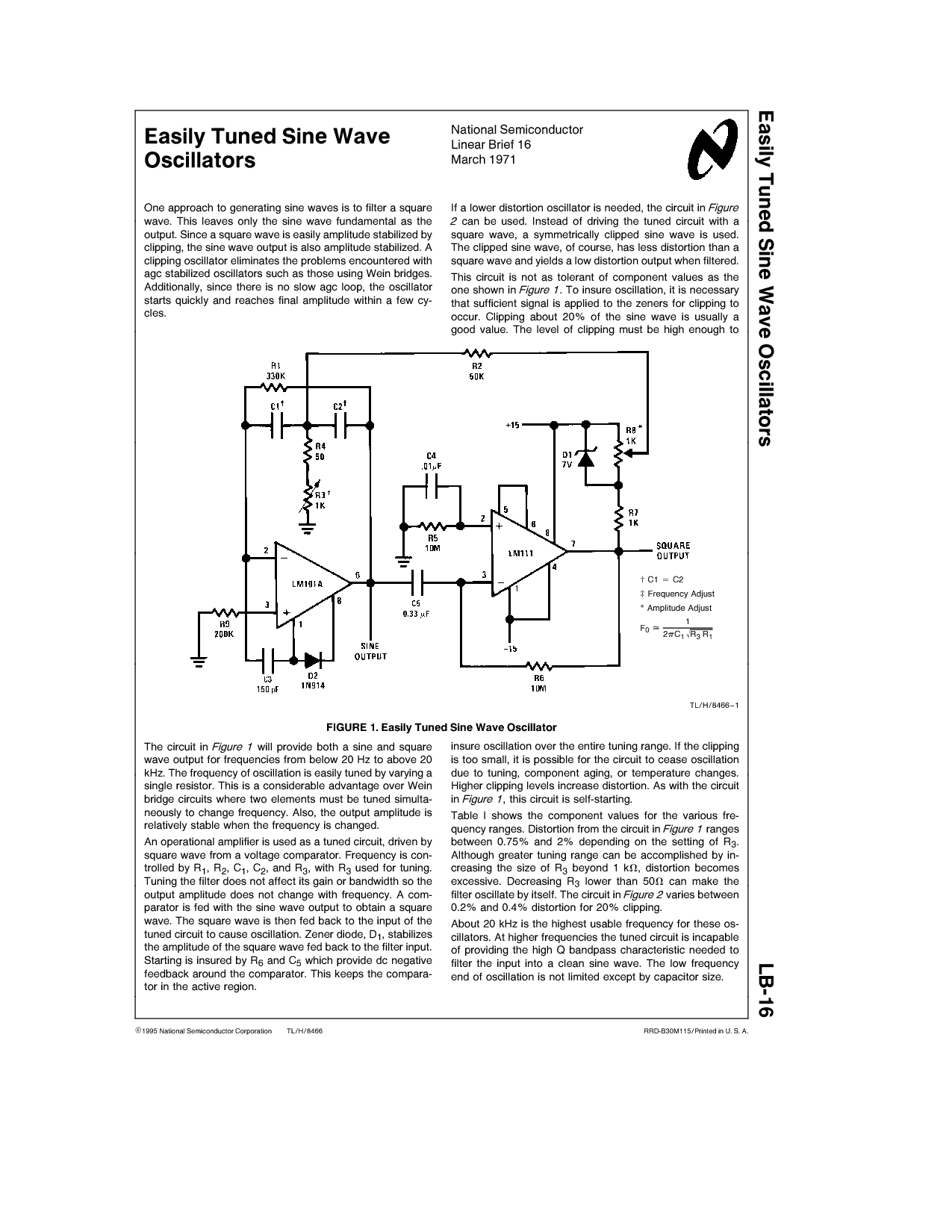
One approach to generating sine waves is to filter a square wave. This leaves only the sine wave fundamental as the output. If a lower distortion oscillator is needed, the circuit in Figure 2 can be used. Instead of...
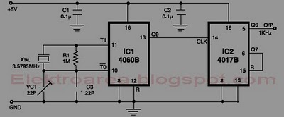
This circuit is designed for accurate time-base generation utilizing the commonly available 3.5795 MHz crystal, which is frequently used in telecommunication equipment. A crystal-based oscillator combined with a divider IC chain or a similar circuit, such as an ASIC,...