
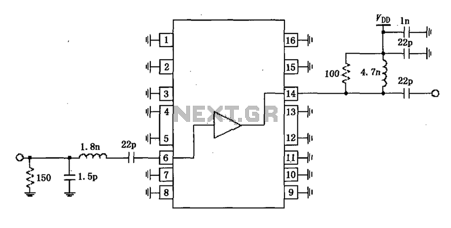
Boss DM-2 Delay Guitar Pedal Schematic Diagram

This circuit, commonly referred to as the DM-2, has undergone multiple revisions, each aimed at improving performance characteristics while maintaining functionality. The original design incorporated the MN3005 Bucket Brigade Device (BBD) in conjunction with the MN3101 clock driver, which served as the timing mechanism for the BBD. The PCB for this version is marked ET5214-510.
In subsequent iterations, modifications were made to enhance the circuit's efficiency and sound quality. The introduction of the MN3102 clock driver replaced the MN3101, offering improved performance metrics. Additionally, the transition from the MN3005 to the MN3205 BBD, which is a low current variant, was implemented. The PCB markings for these newer versions are ET5214-510A and ET5214-510B.
The MN3205, while slightly noisier than its predecessor, provides a notable reduction in distortion levels, measuring at 0.8% compared to the 1% distortion associated with the MN3005. This reduction in distortion is critical for applications requiring high fidelity audio reproduction, as it contributes to a cleaner sound output.
Overall, the evolution of the DM-2 circuit highlights a continuous effort to refine audio performance through component selection and circuit design adjustments, ensuring that each version meets the demands of users seeking high-quality sound modulation.There are at least 3 different versions of this circuit. The first DM-2 version was using the MN3005 BBD and the MN3101 Clock Driver IC (PCB marking: ET5214-510). Later they changed the clock driver to MN3102 and the BBD to the low current version of the same circuit, the MN3205 (PCB markings: ET5214-510A an
d ET5214-510B). The MN3205 is a little noisier, but it generates less distortion (only 0. 8% compared to 1% for the MN3005). 🔗 External reference
Related Circuits
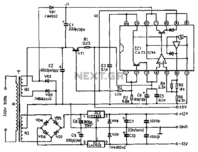
The circuit depicted features a secondary N3 center tap transformer (T) with a common point connecting diodes VD2 and VD3 to positive electrodes, along with capacitors C2, C6, C7, and negative electrodes connected to capacitors C9 and C10. Additional...
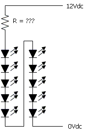
The color of the LED makes a significant difference. The type and size of the LED, such as 3mm or 5mm, and the power source are crucial factors to consider. More information is required for accurate calculations. A basic...
This power supply utilizes a single 7812 IC voltage regulator along with multiple external pass transistors, enabling it to deliver output load currents of up to 30 amps. The circuit design incorporates a 7812 linear voltage regulator, which is...
The metal detector circuit consists of a probe oscillator, a PLL (phase-locked loop) circuit, and an audio alarm circuit. The probe oscillator includes a detection coil (L), transistor (V1), and several resistors (R1 to R3) and capacitors (C1 to...
A narrowband linear amplifier circuit configured with the RF2320 operates within a frequency range of 1930 to 1990 MHz. The radio frequency (RF) signal is input from a distance of 6 feet and is amplified by an internal amplifier...
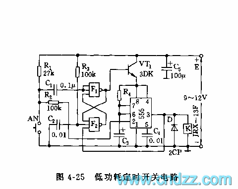
555 low power timing circuit diagram. The diagram is from the technical information of Chinaicmart. For more detailed information about the circuit diagram. The 555 timer IC is widely utilized in various applications due to its versatility and ease of...