
1930 ~ 1990MHz narrow-band RF2320 linear amplification circuit diagram

The described narrowband linear amplifier circuit utilizes the RF2320, which is specifically designed for high-frequency applications. The operational frequency range of 1930 to 1990 MHz makes it suitable for various RF communication systems. The input RF signal is received from a distance of 6 feet, where it is amplified through the internal amplifier positioned 14 feet from the input source.
The direct coupling of the internal amplifier to the input signal path is an essential design choice, as it minimizes signal loss and preserves the integrity of the RF signal. However, this configuration requires the integration of a blocking coupling capacitor to prevent DC components from affecting the amplifier's performance. The typical gate voltage at the input terminal is set to 0V, establishing a baseline for signal amplification. Increasing the external gate bias voltage will lead to a rise in the output current; however, it is crucial to note that this adjustment does not enhance the linearity of the amplifier, which is a critical parameter in RF applications to ensure signal fidelity.
The output of the amplifier, located 14 feet away, is designed to provide both the amplified RF signal and the necessary internal bias. The absence of DC blocking capacitors within the RF2320 chip necessitates the use of an external 22pF capacitor. This capacitor serves as a DC blocking element, allowing only the AC components of the amplified signal to pass while preventing any DC offset from affecting downstream components.
To optimize performance, an output matching network is implemented to align the output impedance of the amplifier with the load impedance. This matching network is vital for achieving maximum output power and efficiency, which are critical for effective RF signal transmission. By ensuring that the amplifier is properly matched to its load, signal reflections are minimized, and power transfer is maximized, leading to improved overall system performance.1930 ~ 1990MHz as shown in Fig narrowband linear amplifier circuit configured by RF2320. Radio frequency (RF) signal input from 6 feet, after amplified by an amplifier 14 feet out. 6 feet and internal amplifier is directly coupled, so plus a blocking coupling capacitor. Typically, the gate voltage of the input terminal is 0V, but the external gate bias voltage increases will increase, which will increase while the current, but will not improve amplifier linearity. 14 feet while providing outputs and internal bias, not in the chip DC blocking capacitors, and the pin dc voltage, so a 22pF capacitor as a DC blocking capacitor.
Output matching network to match the output impedance of the amplifier, in order to obtain the maximum output power and efficiency.
Related Circuits
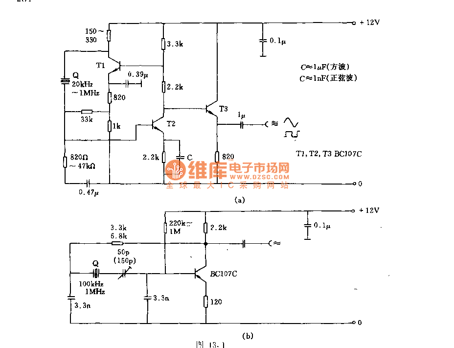
Figures (a) and (b) illustrate two basic oscillator circuits operating at 2 MHz. The circuit design allows for adjustment of the optimal operating point through testing. The two oscillator circuits depicted in the figures utilize different configurations to achieve stable...
The voice circuits discussed in this section operate such that during daylight or in bright conditions, the voice-activated switch remains off, preventing the lamp from lighting. Conversely, in low-light conditions or at night, the sound control switch is activated....
This circuit functions as a camera switch, allowing multiple cameras to be connected to a single monitor. It can operate in both manual and automatic modes. In automatic mode, the circuit utilizes a 555 astable multivibrator to generate a...
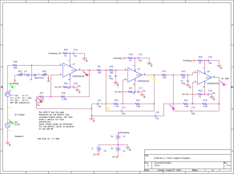
A bandwidth-limited amplifier shapes the waveform sampled by the 40 MHz high-speed pipeline Analog to Digital Converter (fast ADC, or fADC). It is well known that the shaping time is twice the time constant (peaking time) for each pole...
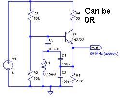
An oscillator circuit capable of generating a high-quality sine wave with a frequency of at least 500 MHz, intended for RFID applications. There have been attempts to utilize a class E oscillator, but the design has not yet been...
Often, there is a need for an additional telephone ringer in an adjacent room to indicate an incoming call. For instance, if the telephone is located in the drawing room, an extra ringer may be required in the bedroom....