
Buck Boost converter using LTC3440 for an output voltage of 3.3 volts
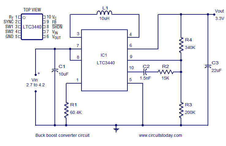
The LTC3440 is a synchronous buck-boost converter designed for applications requiring a stable output voltage from a varying input voltage. This device is particularly useful in battery-powered applications where the input voltage may fluctuate as the battery discharges.
The buck-boost topology allows the converter to step down (buck) or step up (boost) the input voltage to maintain a constant output voltage of 3.3V. This is achieved through the use of two internal power switches (one for bucking and one for boosting), which are controlled by a pulse-width modulation (PWM) scheme. The switching frequency can typically be set to optimize efficiency and minimize component size.
In this configuration, the input voltage of 2.7V to 4.2V is connected to the input pin of the LTC3440. The output pin is connected to the load, which requires a stable 3.3V supply. The converter's feedback loop continuously monitors the output voltage and adjusts the duty cycle of the PWM signal to regulate the output voltage effectively.
Key components that may be included in this design are input and output capacitors, which help to filter voltage spikes and maintain stability during load transients. Additionally, an inductor is required to store energy and facilitate the conversion process, while diodes are used to direct the current flow appropriately during the switching cycles.
Overall, the LTC3440 buck-boost converter provides a compact and efficient solution for applications needing a regulated output voltage, ensuring reliable performance across a wide range of input voltages.A simple a very efficient buck boost converter implemented using LTC344o IC . The output voltage is 3.3V and input can be between 2.7 to 4.2 volts.. 🔗 External reference
Related Circuits
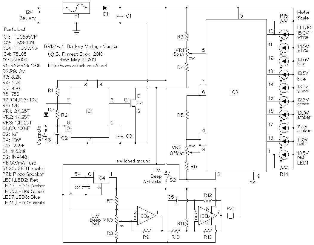
This circuit provides an audible and visual low voltage warning for 12V battery powered devices. When the battery voltage is above the set point (typically 11V), the circuit is idle. If the battery voltage should fall below the set...
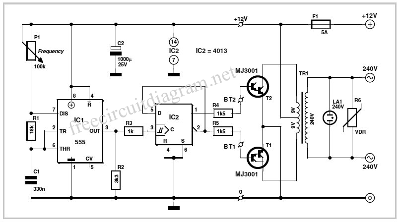
This circuit diagram for a 12V inverter is simple to construct and utilizes inexpensive components that many electronics hobbyists may already possess. While it is feasible to create a more powerful circuit, the complexity arises from managing the significant...
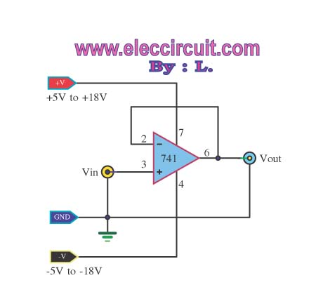
The buffer operational amplifier (op-amp) circuit is utilized for coupling two circuits together. It functions as a unity gain follower, also known as a voltage follower, which is employed to transfer or replicate a voltage from one circuit to...
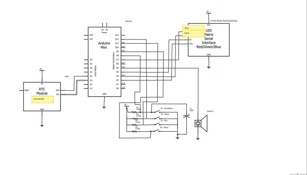
The device is designed to promote respectful time management during meetings, particularly useful in ship-room or SCRUM meetings. The following is a list of components required, including links for purchasing specific parts. It is advisable to check eBay or...
This design is based on an 18 Watt audio amplifier and was developed primarily to meet the needs of users who are unable to find the TLE2141C chip. It utilizes the widely available NE5532 dual integrated circuit; however, its...
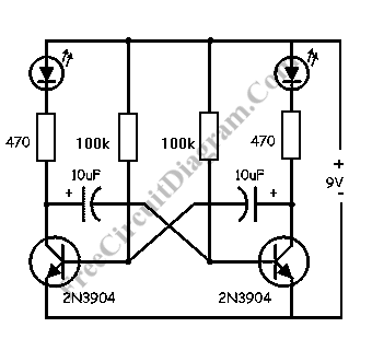
This LED flasher circuit is a classic two-transistor flip-flop. It is a popular circuit often built by beginners in electronic circuit design. The schematic diagram of this well-known LED flasher circuit consists of two transistors, two capacitors, four resistors,...
Warning: include(partials/cookie-banner.php): Failed to open stream: Permission denied in /var/www/html/nextgr/view-circuit.php on line 713
Warning: include(): Failed opening 'partials/cookie-banner.php' for inclusion (include_path='.:/usr/share/php') in /var/www/html/nextgr/view-circuit.php on line 713