
Butler emitter follower oscillator 100Mhz

The circuit under discussion utilizes an emitter follower configuration, which is a type of transistor amplifier that provides voltage gain close to unity (1). The primary function of this configuration is to buffer the input signal, ensuring that the output can drive a load without significantly affecting the input signal's voltage.
In this design, the emitter follower employs negative feedback, which plays a crucial role in stabilizing the gain. Negative feedback occurs when a portion of the output signal is fed back to the input in a manner that opposes the input signal. This process helps to minimize the effects of any parasitic elements that may arise from the circuit components, thereby enhancing the overall performance and reliability of the circuit.
The emitter follower configuration typically consists of a bipolar junction transistor (BJT) or a field-effect transistor (FET) with its emitter (or source) connected to the output. The base (or gate) receives the input signal, while the collector (or drain) is connected to the power supply. The output is taken from the emitter (or source), which provides a low output impedance, making it suitable for driving capacitive loads or other stages in a circuit.
In summary, this circuit achieves effective signal buffering with a gain of one while utilizing negative feedback to stabilize performance and mitigate the impact of parasitic elements. This design is particularly useful in applications where signal integrity and stability are paramount, such as in audio processing, sensor interfacing, and other analog signal conditioning tasks.This circuit has good performance without amplifier has a gain of only one with built-in any parasitics because emitter follower negative feedback to stabilize its gain.
Related Circuits
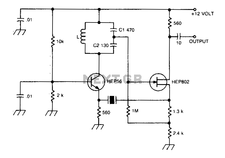
A typical Butler oscillator operating within the frequency range of 20 to 100 MHz incorporates a Field Effect Transistor (FET) in the second stage of its configuration. The circuit exhibits reliability issues when utilizing two bipolar transistors. In some...
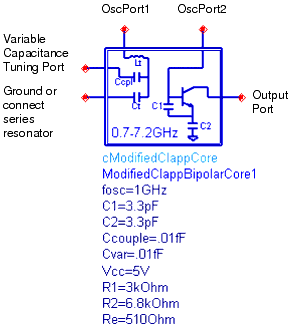
The Oscillator Design Guide is integrated into Agilent EEsof's Advanced Design System environment, functioning as a smart library and interactive handbook for the creation of effective designs. It facilitates quick oscillator design, interactive component characterization, and provides in-depth insights...

The circuit operates as a unijunction transistor relaxation oscillator. The base of the lower PNP transistor is biased at approximately half of the supply voltage. As the 100pF capacitor charges through the 1GΩ resistor, the base of the upper...
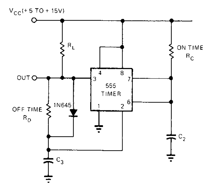
The 555 timer circuit has unsteady open and closing times that are independent of one another. One time constant is given by 1.1RcC2, while another time constant is defined as 1.1RcC3. The free-running period is the sum of these...
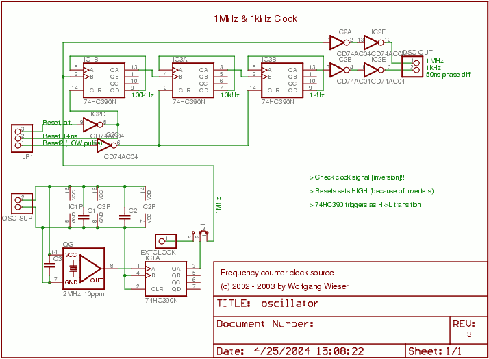
The oscillator generates a 1 MHz and a 1 kHz clock signal. The 1 MHz clock serves as the primary clock for the microcontroller and provides a time base for millisecond measurements. A 2 MHz signal is divided by...
This gated 1-kHz oscillator provides press-to-turn-off functionality, along with waveforms available at the output of pin 3 and across capacitor C1. The gated 1-kHz oscillator circuit is designed to generate a square wave output at a frequency of 1 kHz....