
Car Door Keypad Using Lin

The CDCF5801 is a versatile clock management device designed for applications requiring precise clock signal manipulation. It features advanced clock multiplication and division capabilities, allowing it to generate output frequencies that are critical in high-speed digital systems. The device's phase aligner function is particularly noteworthy, enabling fine-tuning of clock signals with a resolution of 1.3 mUI, which is essential for maintaining signal integrity in high-performance applications.
The architecture of the CDCF5801 includes multiple input and output configurations, with two main outputs, CLKOUT and CLKOUTB, capable of being configured for single-ended or differential signaling. This flexibility allows the device to interface with various signaling standards, including LVDs, LVPECL, and HSTL/SSTL, making it suitable for a wide range of digital communication applications.
The pre-divider and post-divider functionalities provide further customization of output frequencies, allowing designers to select from a range of multiplication and division ratios. This adaptability is crucial for meeting the specific frequency requirements of different systems while ensuring minimal jitter transfer from input to output.
Power management features, including selectable power-down and high-impedance modes, enhance the device's usability in power-sensitive applications. The ability to adjust the common-mode range of the REFCLK input by varying the VDDREF voltage increases the overall robustness of the device in various operating environments.
Overall, the CDCF5801 is designed to deliver high performance, low jitter, and flexible clock management solutions for advanced electronic systems, ensuring reliable operation across a wide temperature range and diverse applications.The CDCF5801 provides Clock multiplication from a reference Clock (REFCLK) signal with the unique capability to delay or advance the CLKOUT/CLKOUTB with steps of only 1. 3 mUI through a phase aligner. For every rising edge on the DLYCTRL pin the CLKOUT is delayed by a 1. 3-mUI step size as long as the LEADLAG input detects a low signal at the time o f the DLYCTRL rising edge. Similarly for every rising edge on the DLYCTRL pin the CLKOUT is advanced by a 1. 3-mUI step size as long as the LEADLAG pin is high during the transition. This unique capability allows the device to phase align (zero delay) between CLKOUT/CLKOUTB and any one other CLK in the system by feeding the Clocks that need to be aligned to the DLYCTRL and the LEADLAG pins. Also it provides the capability to program a fixed delay by providing the proper number of edges on the DLYCTRL pin, while strapping the LEADLAG pin to dc high or low.
Further possible applications are: Aligning the rising edge of the output Clock signal to the input Clock rising edge Avoiding PLL instability in applications that require very long PLL feedback lines Isolation of jitter and digital switching noise Limitation of jitter in systems with good ppm frequency stability The CDCF5801 provides Clock multiplication and division from a reference Clock (REFCLK) signal. The device is optimized to have extremely low jitter impact from input to output. The predivider pins MULT[0:1] and post-divider pins P[0:2] provide selection for frequency multiplication and division ratios, generating CLKOUT/CLOUTKB frequencies ranging from 25 MHz to 280 MHz with Clock input references (REFCLK) ranging from 12.
5 MHz to 240 MHz. The selection of pins MULT[0:1] and P[1:2] determines the multiplication value of 1, 2, 4, or 8. The CDCF5801 offers several power-down/ high-impedance modes, selectable by pins P0, STOPB and PWRDN. Another unique capability of the CDCF5801 is the high sensitivity and wide common-mode range of the clock-input pin REFCLK by varying the voltage on the VDDREF pin.
The Clock signal outputs CLKOUT and CLKOUTB CAN be used independently to generate single-ended Clock signals. The CLKOUT/CLKOUTB outputs CAN also be combined to generate a differential output signal suitable for LVDs LVPECL, or HSTL/SSTL signaling.
The CDCF5801 is characterized for operation over free-air temperatures of -40C to 85C. 🔗 External reference
Related Circuits
The code in mikroC PRO for the PIC16F887 microcontroller is designed to operate with an 8.000 MHz clock frequency on a Microchip 44-pin demo board. The routines have been developed using HITECH C, but the focus is on utilizing...

Blinking an LED is the introductory project for programming microcontrollers. It serves as an effective method to navigate the entire development process and verify the functionality of all tools. This chapter involves connecting a light-emitting diode (LED) to an...
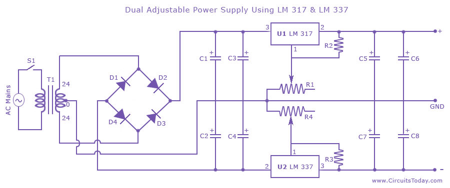
Dual adjustable power supply circuit with a diagram using IC LM317 and LM337. This variable power supply circuit has a range of 1.2 volts to 30 volts. The dual adjustable power supply circuit utilizes the LM317 and LM337 voltage regulators...
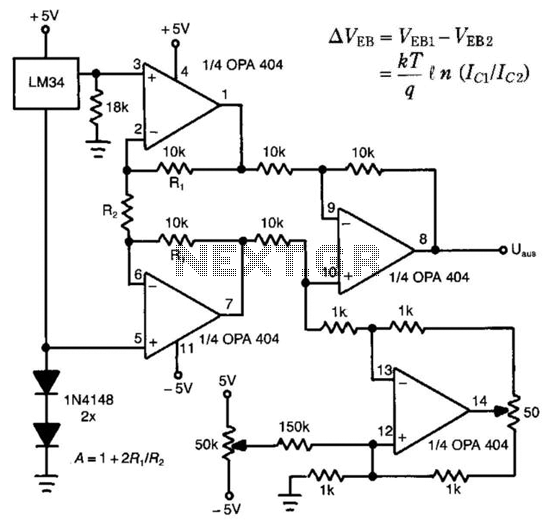
The LM34 is utilized as a sensor in the design of this linear thermometer. Its output represents the difference between two base-emitter voltages (Veb) of two transistors that operate at different collector-current densities. These current densities are denoted as...
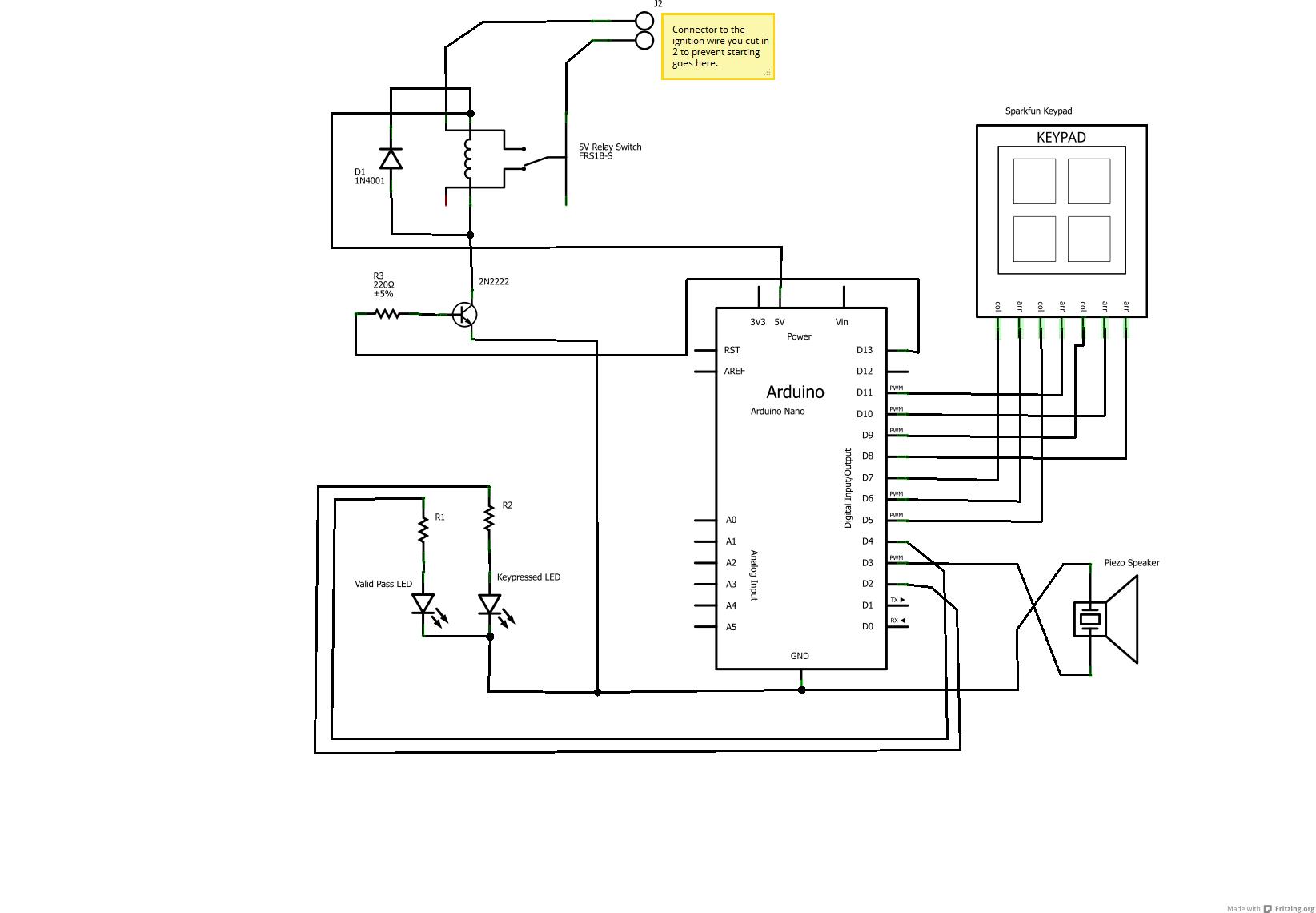
Audible signals will alert if the password or keycode entered is accepted or not (in this case, random sounds for incorrect entries and the Super Mario theme for success) using a standard piezo speaker. The under-dashboard USB hub is...
Climber A ascends a route while Climber B remains on the ground, tracking Climber A's progress with a laser pointer. The Redpointer device records the exact route taken. In Mode 1, the recorded route is played back in real-time,...