
CAR IMMOBILIZER CIRCUIT

This results in a corresponding increase in the voltage at the emitter of Q2. The Darlington pair configuration is utilized to create a high input impedance buffer stage, allowing the voltage across C2 to increase towards near full power without being limited by loading effects, which would otherwise impose a few volts of burden. Eventually, the voltage applied to the relay reaches a level sufficient to enable it, closing the contacts and shorting the points. Consequently, the ignition system fails to operate correctly, resulting in the vehicle being inoperable. When the ignition is turned off, power is removed from the circuit, and diode D1, which is reverse-biased, becomes polarized by the charge from C1. Diode D1 permits C1 to discharge rapidly through resistor R2 and all other current paths through the supply lines. The circuit is set to operate again when the ignition is turned on. The engine runs, but not for an extended period. The values of R1 and C1 create a delay of approximately 25 to 30 seconds. Increasing the value of R1 extends this delay.
The circuit design incorporates a flip switch mechanism that activates the system when the ignition switch is engaged. The power management is critical, as the circuit remains dormant until the ignition is turned on, ensuring energy efficiency. The charging of capacitor C1 initiates the operation of the Darlington pair, which is essential for amplifying the input signal while maintaining high input impedance. This configuration prevents loading effects that could compromise the performance of the circuit.
The relay K1 plays a pivotal role in controlling the ignition system. By remaining open initially, it ensures that the vehicle's ignition system is unaffected until the necessary voltage threshold is reached. The gradual increase in voltage across C1 and subsequently at the base of Q1 is a crucial aspect of the timing mechanism that determines when the relay activates.
Diode D1 is strategically placed to manage the discharge of C1 when the ignition is turned off, allowing for a swift reset of the circuit. This feature is vital for ensuring that the system is ready for the next ignition cycle without delay. The timing characteristics, governed by the resistor R1 and capacitor C1, can be adjusted to suit specific operational requirements, providing flexibility in the system's response time. The overall design emphasizes reliability and efficiency, making it suitable for automotive applications where precise control over the ignition system is necessary.A flip of 51 puts the system in action. Power for the circuit is captured from the ignition switch, and circuit receives no power until the ignition switch is closed. When the camera is turned on, the capacitor C1 is charged and the emitter follower Darlington pair (formed by Q1 and Q2) are cut, so no voltage is applied to the relay (Kl), which serves as a load QL transmitter.
normally open relay contacts are connected through the points of the vehicle. (At this point, the relay contacts are open and have no effect on the ignition system). Cl charges through R, causing the voltage at the base of Ql to rise steadily. This creates a similar increase in the voltage at the emitter of Q2. A Darlington pair is used to provide a high input impedance buffer stage so that the voltage across C2 is free to increase the potential of near full power. effects of loading does not limit the potential burden of a few volts. Finally, the voltage applied to the relay becomes sufficient to enable it. Close contacts and short points. The ignition system now does not work properly and the vehicle is down. If the ignition is off, power is removed from the circuit and the diode Dl, which used reverse-biased, has become polarized by the charge of C1.
Dl allows C1 to discharge rapidly through R2 (and all other routes current through supply lines). The circuit is ready to operate when the ignition is on again. The engine works, but not for very long. The values of R1 and C 1 has a delay of about 25 to 30 seconds. Increasing the value of R1 to provide a longer period.
Related Circuits

The SLB0586A integrated circuit from Siemens can be utilized to construct a straightforward touch light dimmer circuit, enabling the adjustment of lamp intensity. When paired with a TIC206D triac, this setup allows for smooth regulation of light intensity for...
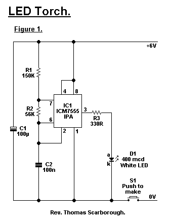
A common issue with small flashlights is the limited lifespan of both the batteries and the bulb. For example, a typical incandescent flashlight consumes approximately 2 Watts, while the LED flashlight shown in Fig. 1 consumes only 24 mW....
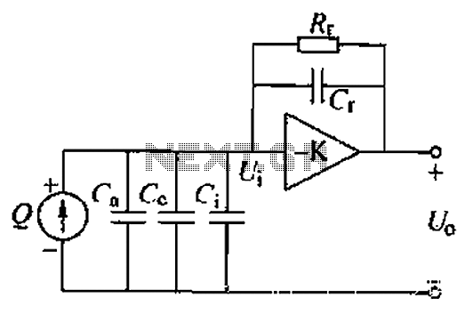
A charge amplifier is an effective device for measuring punch hits. This amplifier utilizes a negative feedback capacitor in conjunction with a high-gain operational amplifier. The amplifier operates with minimal shunt, relying primarily on the feedback capacitor's charge (q...
When the door is pushed, a whisper is heard that transitions to a higher frequency. The oscillator frequency is determined by the audio frequency coupling capacitance, C1, and the resistance connected between the base of transistor Q1 and ground....
The circuit is designed to stabilize the brightness of lamp L using a thyristor-based AC automatic voltage regulator. The thyristor T5 is connected diagonally across the bridge circuit. The trigger pulses are generated by components VT1, VT2, and VT3,...
The circuit operates using an integrated circuit (IC) NE555 along with resistors R, RP, and capacitor C3, forming an astable multivibrator configuration. The output from pin 3 of the IC generates a square wave oscillation signal, which is passed...