
Cd Ignition System For Autos Circuit

The CD4-MX circuit is designed to efficiently convert a low-frequency signal into a high-voltage output suitable for igniting an automotive ignition coil. The astable multivibrator configuration formed by Q1 and Q2 generates a continuous square wave, which drives the primary winding of transformer T1. The step-up transformer is critical as it increases the voltage to a level sufficient for ignition purposes.
The rectification stage, comprised of diodes D3 to D6, ensures that the alternating current output from the transformer is converted to direct current, which is then stored in capacitor C4. This storage allows for a quick release of energy upon the activation of SCR1. The firing of SCR1 is controlled by a voltage signal from the ignition points, which acts as a trigger. When the points close, the voltage applied to the gate of SCR1 allows it to conduct, effectively transferring the charge from C4 to the ignition coil, resulting in a spark necessary for engine ignition.
To accommodate different ignition systems, the circuit includes provisions for non-point breaker configurations through terminals X15+ and X15-. In such cases, the unused resistor R6 must be removed to prevent interference with the operation. The use of optocoupler U1 provides additional flexibility by allowing for isolation between the control signals and the high-voltage output, with its configuration depending on the polarity of the sensor used.
The design emphasizes safety, particularly given the potential output voltage of 60 to 70 kV. Proper safety measures, such as using insulated tools and ensuring that the circuit is not live during adjustments, are critical to prevent electrical hazards. Overall, the CD4-MX circuit is a versatile ignition system capable of adapting to various automotive applications while delivering reliable performance. At the heart of the CD4-MX is an astable multivibrator, built around Q1 and Q2, that feeds step-up transformer Tl. The output of 1 is rectified by D3 to D6 and used to charge capacitor C4. When the points close, a small voltage is fed to the gate of SCR1, causing it to fire, dumping the charge of C4 to the vehicle`s ignition coil.
The circuit also contains optional subcircuits to accommodate different types of auto ignitions.Xl5 + and X15 - are alternative trigger configurations for nonpoint breaker ignition systems. R6 is not used for these systems and must be removed. Optocoupler Ul can be used (pin 4) in conjunction withX15 - orXI5 + depending on polarity of sensor. Note that 60 to 70 kVis available from this system,,so observe suitable safety precautions.
Related Circuits

This solar charge controller integrates multiple features into a single design, including a 3A current rating, low dropout voltage (LDO), and a range of voltage adjustment capabilities. The solar charge controller is a critical component in solar energy systems, tasked...
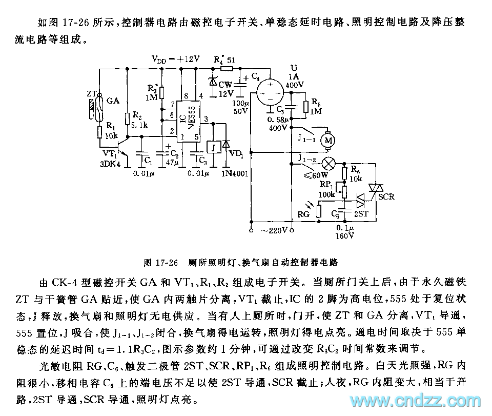
The electronic switch consists of the CK-4 type magnetic control switch and the components VT1, R1, and R2. When the bathroom door is closed, the permanent magnet ZT and the reed switch GA come into proximity, which separates the...
A 555 timer and a dual 556 timer are used to generate a basic video signal, as illustrated in the schematic. The first timer operates in astable mode, producing synchronization pulses with a period ranging from 4.7 to 8...
This circuit simulates a breathing or pulsing LED using a 555 timer chip. It has gained popularity, receiving numerous comments and emails from users who successfully built the circuit, as well as feedback from those who encountered difficulties when...
The function of the sound level display circuit is to enhance the appearance of an amplifier circuit or a radio player. It provides an impressive visual representation of audio levels. The sound level display circuit serves as a visual indicator...
FET relay circuit 2 is essentially a JS-20 time relay circuit. When the switch SA is open, the relay device KA remains in the released state. Once switch SA is closed, the delay period begins. After a specified duration,...