
CD4060 production time controller circuit diagram

The CD4060 integrated circuit serves as a versatile timer and oscillator, leveraging both its counter functionality and oscillator capabilities. The circuit operates by generating a square wave signal through an external resistor (R5) and capacitor (C3), which determines the frequency of oscillation. The counter counts the oscillations, and the output at pin 14 signifies the completion of a predetermined count.
The transition of the output from low to high at pin 14 activates the subsequent components in the circuit. The transistor V acts as a switch, controlling the current flow to relay K. When the output is low, the transistor is turned off, preventing current from flowing through the relay coil and keeping the load de-energized. As the output transitions to high, the voltage across R6 ensures that the transistor is driven into saturation, allowing maximum current to flow through the relay coil, thus closing the relay contacts and energizing the load.
The adjustable delay time, achieved through the selection of R5 and C3 values, allows for flexibility in timing applications. The circuit can be configured for various time delays, making it suitable for applications requiring precise timing control, such as in industrial automation, home appliances, or any system requiring delayed activation of a load. The range of 2.1 to 4 hours provides a significant window for adjustment, accommodating different operational needs. Overall, this CD4060-based time controller circuit exemplifies a practical solution for timing and control applications in electronic systems.With a CD4060 shown below production time controller circuit connected instantly, guaranteed by R5, C3 constitute a differential circuit delay time from scratch. Under the action of the oscillating signal, the counter starts work CD4060 within 3 feet for the first output of the counter 14, to make 3 feet from low to high level, the time required for t = 213 2.2KC (seconds), low voltage output during this period of 3 feet off the transistor V. When the delay time comes, jump 3 feet from low to high, so that by limiting R6 V saturated conduction, the relay pull-K, the load is energized.
The circuit delay time within 2.1 to 4 hours to be adjusted.
Related Circuits

This circuit diagram of a digital clock utilizes six common anode seven-segment displays to indicate the time. It does not require microcontrollers or PICs for operation. The circuit operates using the MM5314 integrated circuit, functioning at either 50 Hz...
Frequency meter circuit for service applications, including all standard frequency bands: amateur HF, VHF, and UHF, displayed on an LCD screen. The frequency meter circuit is designed to accurately measure and display frequency across various amateur radio bands, specifically HF...

The diagram illustrates the connections for the inputs and outputs of each operational amplifier from the power source, detailing how each operational amplifier is configured to operate individual light-emitting diodes (LEDs). It also includes calculations for determining each resistor...

A momentary contact push button switch can be utilized to conveniently turn the Raspberry Pi (RPi) ON and OFF. Pressing the button will apply power to the micro USB header, maintaining power while the Raspberry Pi initializes and starts...
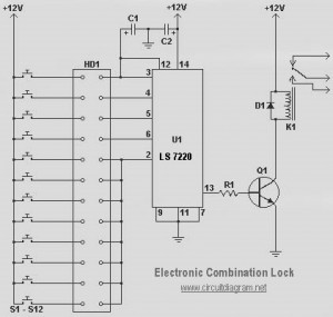
This circuit diagram represents a simple electronic combination lock utilizing the IC LS7220. The circuit is designed to activate a relay for controlling any device (on and off) each time a specific combination of four digits is entered. It...
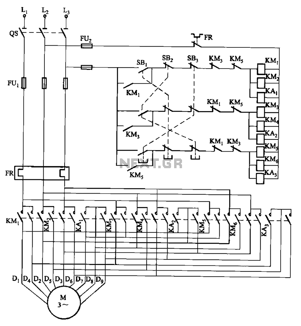
The circuit depicted in Figure 3-115 utilizes contactors and double buttons, allowing for speed conversion without the need to press the stop button. The buttons SBi, SBz, and SB3 correspond to high, medium, and low-speed operation, respectively. This circuit design...