
Circuit transmits ARINC 429 data

The ARINC 429 standard is crucial for reliable data transmission in aviation systems, utilizing a carefully designed physical layer to ensure signal integrity. The chosen 78Ω shielded twisted-pair cable minimizes electromagnetic interference (EMI) and crosstalk, which is essential in the electrically noisy environments typical of aircraft. The differential signaling method, employing a return-to-zero (RZ) waveform, enhances noise immunity by allowing the receiver to detect the difference between two voltage levels, effectively reducing the impact of common-mode noise.
The circuit architecture centers on a FIFO memory configuration, specifically IC1, which facilitates the buffering of data before transmission. The FIFO's capability to hold multiple words allows for smooth data flow from the microcontroller's SPI interface, ensuring that the ARINC data stream is outputted at the required baud rate. The 100 kHz baud rate is derived from a 1 MHz clock signal, which is divided down to meet the ARINC specification. The use of additional logic gates, such as IC3A and IC3B, ensures that the data readiness and timing requirements are strictly adhered to, preventing data loss or transmission errors.
The multiplexer IC4 plays a pivotal role in generating the appropriate output waveforms by gating the necessary voltage levels (–5V, 0V, 5V) in accordance with the ARINC 429 protocol. The LRC network at the output is designed to shape the rise and fall times of the output signals, ensuring compliance with the ARINC 429 timing specifications. This careful design consideration is vital for maintaining the integrity of the transmitted signals, which must meet strict timing requirements to be compatible with other aircraft systems.
The process of converting five 8-bit SPI bytes into a single 32-bit ARINC 429 word involves a systematic approach to data organization. The structure of the 32-bit word is defined, with each byte contributing specific information. This organization is critical for downstream systems that rely on correctly formatted ARINC 429 messages for communication and data exchange in avionics applications.The physical transmission medium for the 429 standard is 78Ω shielded, twisted-pair cable that uses a complementary, differential bipolar RZ (return-to-zero) waveform (Figure 2). The voltages are the net differentials that the biphase drive develops: For example, the differential is 10V when you drive the Data A signal in Figure 1 to 5V and the Data B signal to –5V.
In addition to the signal levels, a 429 system must closely control the rise and fall times to conform to the specification. This control limits both intra-cable signal crosstalk and EMI radiation that might interfere with sensitive aircraft communication and navigation systems.
The operation of the transmitter in Figure 1 centers around IC1, a 4-bit×16-word FIFO memory. The serial ARINC bit stream comes from the microcontroller's synchronous serial-peripheral interface (SPI); the C input of IC1 buffers the data stream. In addition, the D input of IC1 serves as a buffered ARINC-enabled bit (the microcontroller's J port, bit 2).
When low, this bit disables the ARINC transmitter logic and permits other system peripherals to use the SPI hardware.
Bits A and B of IC1 go unused. The 100-kHz ARINC high-speed baud rate comes from the 1-MHz reference supplied to the IC3A divide-by-10 circuit. The 100-kHz signal drives IC1's shift-out (SO) pin and the IC2 pulse gate. The presence of bits in the IC1 FIFO (indicated by QR=1) resets the ARINC RDY bit in IC3B and enables IC3A.
If IC1's D bit (Pin 10) is also high, it gates the 100-kHz square wave to the IC4 multiplexer. This action causes the sequential gating of –5, 0, and 5V onto the A/B data-output signals in ARINC-compatible waveforms. The LRC network at the output ensures compliance with the 429 requirements for rise and fall times. The circuit must process five 8-bit SPI bytes to generate each 32-bit, 429-compliant output word. Table 1 shows the format of the SPI bits. The first four bytes in Table 1 combine to form a 32-bit ARINC 429 word. The 32-bit word, reading from right to left, starts with byte 1 (again, reading from right to left), then tacks on byte 2, and so on.
🔗 External reference
Related Circuits

When the circuit is connected to hi-fi equipment or at both ends of the electronic instrument's speaker, the audio level can be modulated to a 500W lamp proportionally. This is achieved using three appropriate sets of audio filters and...
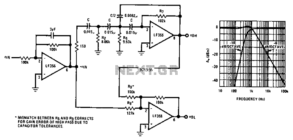
Asymmetric third-order Butterworth active crossover network circuit diagram. The asymmetric third-order Butterworth active crossover network is a sophisticated circuit designed to split an audio signal into two separate frequency bands, typically for use in multi-way speaker systems. This type of...
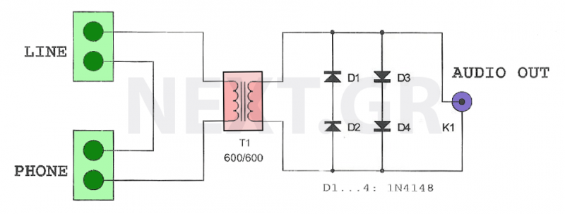
This circuit is designed to record telephone conversations on a landline telephone. It requires a small circuit and a computer subscription. Recording conversations is useful for recalling important discussions. Previously, this was accomplished using a small tape recorder, where...
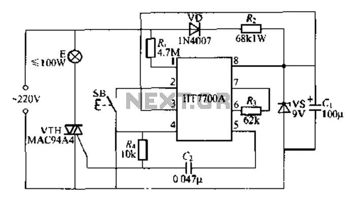
The HT7700A ASIC is designed for stepless dimming of lights, utilizing a single button control mechanism. It offers 96 levels of brightness adjustment. The HT7700A is fabricated using a CMOS process and comes in a standard D1P-S-pin package. The...

A simple 9 Volt, 2 amp power supply utilizing a single integrated circuit (IC) regulator. This circuit is straightforward, as the regulator handles the majority of the work. The component used is the 7809 voltage regulator. The circuit consists primarily...
The battery voltage is 1V for a low-frequency amplifying circuit, which can operate with a power supply voltage ranging from 1V to 1.7V, making it suitable for use with small batteries. The circuit provides an output power of 80mW...