
How To Use A Cmos 4017 To Build A Sequential Timer

The CMOS 4017 decade counter is a versatile component used in various timing and counting applications. This circuit specifically leverages its ability to sequentially activate output pins, which can be utilized in applications such as LED chasers, sound generation, or control of relay-based systems. The design incorporates essential components such as resistors, capacitors, and a transistor to control the timing and current levels effectively. The use of a timing capacitor (C5) allows for controlled sequencing, ensuring that each output pin is activated in a timely manner, which is crucial for applications requiring precise timing sequences.
In terms of implementation, the circuit should be built on a breadboard or PCB, ensuring that all connections are secure and that the power supply is stable. The transistor (Q1) should be selected based on the required current handling capacity for the load being driven, whether it be a relay or a buzzer. The choice of resistors (R1, R5, R11, R12, and R13) should be calculated based on the desired current levels and timing requirements, ensuring that the values are suitable for the operation of the CMOS 4017 and the associated components.
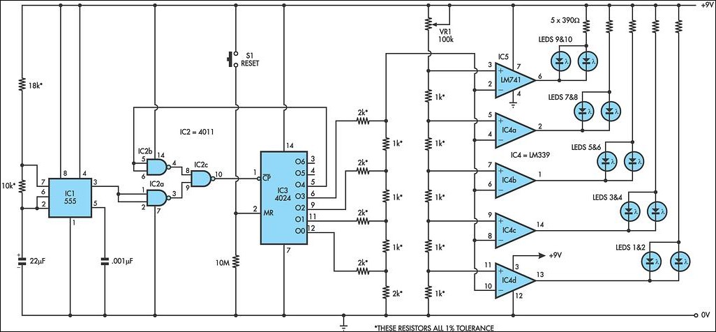
In conclusion, this circuit design effectively demonstrates the use of a CMOS 4017 decade counter for counting applications, highlighting the importance of component selection and timing control in electronic circuits. Proper implementation will yield a reliable and functional counting circuit suitable for various applications.This circuit uses a Cmos 4017. The 4017 is a decade counter. The count starts at zero. And it advances by one - each time pin 14 is taken high. When the count reaches nine - it goes back to zero - and starts all over again. = As the count progresses - each of the output pins goes high in turn. The first is pin 3 - it represents zero. The second is pin 2 - it represents one. Pin 4 represents two - and so on. The number represented by each output pin is shown in red. = Although the 4017 will count up to nine - we are only using it to count up to four. Consequently - some of the output pins are unused. Unused Cmos output pins should always be left unconnected. = The circuit uses the first five outputs. These are - pins 3, 2, 4, 7 & 10 The first four outputs pins are each connected to a 2k7 resistor. With a 12v supply - the resistor limits the current available to 12v G· 2k7 = just under 5mA. = This is more than enough to operate a transistor switch. And the transistor can be used to sound a buzzer - or energize a relay. If you increase the current to about 10mA - it will drive an optical isolator. = To increase the current - you should reduce the value of the resistor. As a rough guide - it`s safe to draw up to about 1mA per supply volt. This means that the value of the resistor - should never be below 1k. = Every step in the sequence is the same. Each output charges C5 through a timing resistor. And - when the voltage on C5 takes pin 14 high - the sequence moves on to the next output. For clarity - I`ve only highlighted the first step in the sequence. Once you understand the first step - you`ll understand the remaining three steps as well. = Consider what happens when we turn on the power. The count begins at zero. In other words - pin 3 will be high. And the rest of the output pins will be low. = Pin 3 does three different jobs. It provides the necessary output current - through R1. It discharges C5 rapidly - through R13 & Q1. And it recharges C5 slowly - through D5 & R5. = It`s true that - at power up - C5 doesn`t need discharging. But it does have to be discharged at the start of every subsequent event in the sequence. = For the count to advance to one - pin 14 must be taken high. A Cmos input pin is high when it`s just over half the value of the supply voltage. As pin 3 charges C5 - the voltage on pin 14 rises. When it reaches roughly 6v5 - the counter will advance to one. And the second event in the sequence will commence. = That is - pin 2 will supply the necessary output current. It will also discharge C5 rapidly - through R13 & Q1. And it will begin the process of taking pin 14 high again - by recharging C5 - through D6 & R6. = It`s the act of taking pin 14 high - that causes the timer to advance to the next step in the sequence. But pin 14 can`t be taken high - if it`s already high. That`s why - at the beginning of each step in the sequence - C5 must be discharged. = The job of discharging C5 is carried out by Q1. When the transistor switches on - it discharges the capacitor rapidly - through R13. = We can`t simply use pin 3 to supply base current to the transistor. If we did - Q1 would remain permanently switched on. As a result - the transistor would hold pin 14 permanently low. Consequently - C5 would never charge - and the sequence would never progress. = When pin 3 goes high - we only want it to supply base current to the transistor for a short period.
We want Q1 to switch on - discharge C5 - and then switch off again. Thus leaving R5 free to recharge the capacitor. = We can achieve this by connecting a capacitor between the output pin and the base of Q1. When pin 3 goes high - C1 is in a discharged state. It will take about 10 seconds or so to charge - through R11 & R12. But while it`s charging - it will supply base current to Q1. And the transistor will switch on. = Once C1 is fully charged - the base current will cease. And the transistor will switc 🔗 External reference
Related Circuits
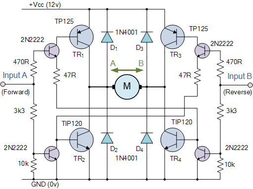
Electronics tutorial about DC motors, electrical motors, and stepper motors used as actuators, including PWM and transistor H-bridge motor control. DC motors, electrical motors, and stepper motors are integral components in various applications, functioning as actuators to convert electrical energy...
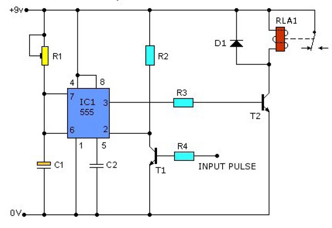
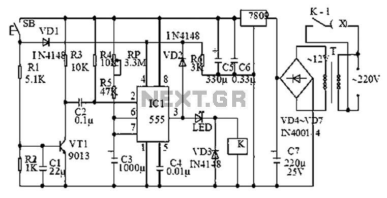
This causes T1 to conduct, pulling pin 2 of IC1 low. IC1 then enters a timing cycle, the duration of which is set by R1 and C1, resulting in pin 3 of IC1 going high. This action causes T2...
This LED circuit replicates the initial LED sequence currently utilized by FISA for Formula One racing. It can also be employed with slot car sets, such as HO scale AFX, Life Like, or Tyco sets, or used in communication-controlled...

The difference between instantaneous frequency and central frequency of the carrier is directly proportional to the instantaneous value of the amplitude of the message signal. A 555 Timer configured in Astable Mode can be utilized for generating Frequency Modulated...
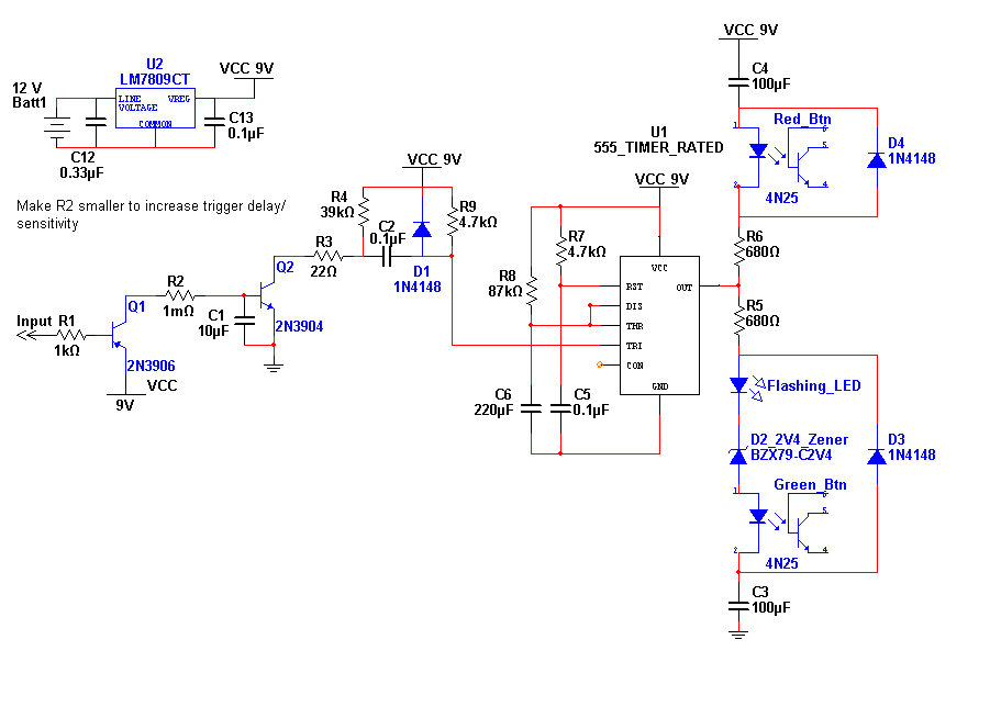
This entry is for the international 555 Contest. The 555 timer chip has been in use for many years and is highly versatile. The concept of this project addresses the need for notification of an event while away from...
The 555 timer is commonly used in time-based circuit designs, particularly in monostable configurations. This setup is straightforward and requires only a few resistors and capacitors to achieve triggering. However, external interference can affect the operation of the circuit...