
fm generation using 555 timer

The described circuit utilizes a 555 timer in astable mode for the generation of frequency-modulated (FM) signals. The operational principle hinges upon the modulation of the control voltage pin, which influences the timing characteristics of the output waveform.
In this configuration, the 555 timer operates by alternately charging and discharging capacitor C1, with the timing determined by resistors R1 and R2. The frequency of the output signal is primarily dictated by the values of these resistors and the capacitor according to the formula fo = 1/(0.693RC). The introduction of the message signal at the control voltage pin modifies the reference levels for the internal comparators of the 555 timer, allowing for dynamic adjustments in the output frequency in response to changes in the amplitude of the input signal.
The circuit's design ensures that when the voltage at the control pin increases, it raises the threshold for the upper comparator, leading to a longer charging cycle for capacitor C1. Conversely, when the control voltage decreases, the time taken to discharge the capacitor is reduced, resulting in a higher frequency output. This modulation process effectively encodes the message signal onto the carrier wave, producing a frequency-modulated signal suitable for various communication applications.
The implementation of diodes and capacitors in conjunction with the 555 timer ensures that the circuit maintains stability and minimizes distortion, which is critical for preserving the integrity of the modulated signal. The careful selection of resistor and capacitor values allows for a wide range of frequency outputs, making this circuit versatile for different modulation requirements. Overall, the application of the 555 timer in this manner illustrates a practical approach to generating FM signals, leveraging its simplicity and reliability in electronic design.The difference between instantaneous frequency and central frequency of the carrier will be directly proportional to the instantaneous value of the amplitude of message signal. 555 Timer wired in Astable Mode can be used for generating Frequency Modulated (FM) waves. Please read the article Astable Multivibrator using 555 Timer for more details about the circuit. In astable multivibrator we don`t use the 5th (Control Voltage) pin of 555 but here we fed the message signal to this pin which results in the variation of frequency. 8th and 1st pin of the 555 are used for giving power, Vcc and GND respectively. 4th pin is the Reset pin which is a active low input, since it is tied to Vcc. When the output is high, capacitor C1 charges to Vcc through R1 and D. When the output is low, capacitor discharges through resistor R2 and 7th of the IC. This charging and discharging time periods determines the time period of output. Message signal is fed to 5th (Control Voltage) pin of the IC through a coupling capacitor and the output can be taken from the 3ed pin of the IC.
I hope that you read the working of Astable Multivibrator using 555 Timer. Central frequency or Carrier frequency of the generated FM can be determined from the expression, fo = 1/(0. 693RC), where R = R1 = R2 and C = C1. When an input voltage (say V) is given to Control Voltage pin, the upper and lower comparator reference changes to voltages V and V/2.
So when the capacitor voltage becomes less than V/2, output becomes high and the capacitor starts charging to Vcc through resistor R1 and diode D. When the the capacitor voltage becomes greater than V, output becomes low and the capacitor starts discharging through resistor R2 and 7th pin of the IC.
So the time period isproportionalto the input voltage V. So as V increases, time period of the output wave increases and when V decreases time period of the output wave decreases. 🔗 External reference
Related Circuits
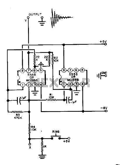
This simple bell circuit utilizes two 555 timers. The frequency is regulated by capacitors that should maintain nearly identical values for optimal performance. Fine-tuning is achieved using resistors R1 and R2. Additionally, the decay time is managed by resistor...
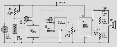
When there is no smoke, the light from the bulb directly illuminates the Light Dependent Resistor (LDR). In this condition, the resistance of the LDR is low, resulting in a voltage drop of less than 6V across it. Consequently,...
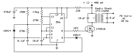
The interval between rings can be adjusted by changing the value of the 1 Meg resistor. A 70 volt, 30 Hz ringing voltage is generated from the 120 volt side of a small 12.6 VAC power transformer (Radio Shack...
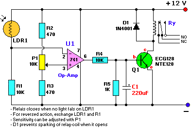
The provided schematic diagram illustrates an LM741 light/dark sensor circuit, derived from the 741 Op-Amp Tutorial by Tony van Roon. The ECG128/NTE128 transistor can be replaced with any NPN transistor that meets the necessary gain and current specifications for...
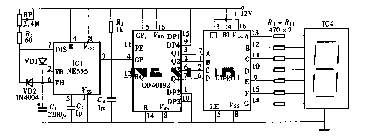
Digital timers feature a clear and precise display. They represent time intervals based on pulse signals, which are decoded by a digital device with a digital display unit. The circuit described pertains to a digital display for these timers,...

The IC555 is an on-chip multivibrator that allows the design of astable, monostable, and bistable multivibrators. Its primary applications include generating timing signals, clock waveforms, synchronizing signals, and square wave oscillators, among others. This document will discuss various applications...