
SSB Modulator

The described circuit represents a sophisticated design for generating single sideband (SSB) signals, integrating various components that contribute to its functionality. The speech amplifier serves as the initial stage, amplifying audio signals before they are processed by the audio phase shift network. The balanced driver circuit ensures that the modulated signals maintain a balanced output, which is critical for reducing distortion and improving signal integrity.
The choice of XR2228 packages as balanced modulators is significant due to their inherent design, which accommodates balanced inputs and outputs, facilitating effective modulation. The operational amplifiers integrated within the XR2228 packages enhance the circuit's performance by providing necessary amplification while maintaining low impedance driving capabilities.
The implementation of trimpots for DC balance adjustments underscores the importance of precision in RF applications. By allowing fine-tuning of the modulator balance, the circuit can achieve optimal carrier rejection, which is vital for maintaining signal clarity and minimizing unwanted artifacts.
The use of flip-flops for generating phase-shifted signals introduces flexibility into the design, enabling the system to adapt to various frequency requirements. This design choice enhances the circuit's versatility, allowing it to operate across a range of frequencies while maintaining the desired phase relationships.
The final output stage, incorporating a low-pass filter, addresses the need to suppress higher order harmonics that may interfere with the intended signal. This filtering is crucial for ensuring compliance with regulatory standards and improving overall signal quality.
Overall, the circuit is a well-thought-out design that balances complexity with functionality, providing a robust solution for generating single sideband signals in the specified frequency range.Circuit detail is shown in figure 3. The main elements of the system are a speech amplifier, the audio phase shift network with balanced driver circuit (N1A, N2A), two balanced modulator stages (N1B & N2B), an RF carrier phase shift circuit (N3) and an output RF driver stage incorporating a lowpass filter (N4). A number of different well known inte grated circuit packages such as the MC1496, NE602 and the SL1640 could have been used as balanced modulators. However I happened to have a number of XR2228 Monolithic Multiplier packages and two of these (N1 & N2) are used for these functions.
These devices have balanced X and Y input circuits, a balanced output and a circuit arrangement which looked ideal for a balanced modulator. They can also handle frequencies up to around 3 MHz, well above our LF range. The XR2228 packages also include an operational amplifier each (N1A & N1B) and the pair of these are used to form a balanced low impedance driver for the audio phase network.
The amplifier outputs are directly coupled through the network to the X inputs of the balanced modulator sections of the packages (N1B & N2B). Precise DC balance of the complete circuit (necessary to set to for best carrier rejection) is set by trimpot RV2.
In retrospect, my thoughts are that it might have been better to use a separate op amp package for the driver as the arrangement resulted in the concentration of a lot of components around the two XR2228 units. Concerning residual carrier balance, a later addition was the inclusion of trimpots RV3 and RV4 which allow individual adjustment balance of the two balanced modulators and further improvement in the rejection of residual carrier.
A 90 degree phase shift for one of the RF carriers can easily be achieved with simple reactive circuits but this system is somewhat confined to a single frequency. Instead, a circuit using two type D or JK flip-flops can provide two outputs 90 degrees apart for any frequency the flip-flops can handle.
For this function, LOCMOS dual JK flip-flop type HEF4027 (N3) has been used. One characteristic of the circuit is that it requires a drive frequency four times the carrier frequency so that for the 160 to 200 kHz transmitter, we need 640 to 800 kHz drive from the VFO. Change between upper and lower sideband is simply achieved by reversing the output leads from N3 which feed the two balanced modulators.
Switch S2 is provided for this purpose. The outputs from the two balanced modulators are combined at the junction of R17 and R20. The single sideband output is insufficient to drive the input of the transmitter and amplifier N4 raises the output level by a factor of 10. The output from the modulators contains higher order frequency components and L1-C8 and R23 -C9 provide a frequency roll-off above 200 kHz to attenuate these components.
This is are the only frequency dependent section of the SSB system, limiting operation much above 200 kHz. Higher order frequency components are further attenuated in the low-pass filter at the output of the transmitter.
As a matter of interest I did carry out some limited tests to see how high a frequency the system could be made to work. (Of course not including the output filters just discussed). I found I could generate single sideband at frequencies as high as 3. 5 MHz, limited probably by the characteristics of the XR2228 packages. I suspect the modulators could be made to go higher using packages such as the NE602. Further to that, higher frequencies could be achieved by heterodyning. The circuit can be switched from SSB to constant carrier for testing or for CW mode by operating switch S1.
It achieves this by unbalancing the modulators to allow carrier to get through. The level of carrier is determined by the degree of unbalance set by trim-pot RV1. The switch also disconnects the speech amplifier so that modulation cannot take place. Whilst I haven`t allowed for it in the 🔗 External reference
Related Circuits
A music-to-light modulator is a circuit which controls the intensity of one or more lights in response to an audio input. The problem in older circuits is that there was a direct electrical connection between the lights using mains...
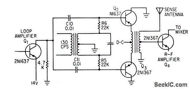
Combines signals from loop and sense antennas of an automatic direction finder to produce a 130-cps output with the correct phase for driving the rotor of a resolver to achieve a null position. The circuit described is integral to the...
The FM modulator circuit, which utilizes frequency modulation, is constructed with a Motorola MC1648P oscillator. It employs two varactors, specifically Motorola MV-209, to achieve frequency modulation of the oscillator. A 5000 Ω potentiometer is incorporated to bias the varactors...
The TBA120 Series integrated circuits (ICs) offer a high-gain limiting intermediate frequency (IF) amplifier and a quadrature coincidence detector in a single package. These ICs are primarily designed for the extraction of television intercarrier sound, which is frequency modulated...
This circuit illustrates an FM modulator with a strong and weak signal switching mechanism. The circuit diagram 3-14 (a) depicts mechanical switches, including a worker selector switch that allows for signal strength selection. Figure 3-14 (b) demonstrates the implementation...
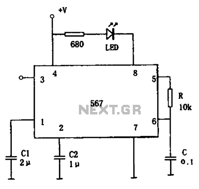
The FM demodulation circuit is illustrated in Figure 567. The FM signal is input at pin 3, and the demodulated signal is output from pin 5. The center frequency of the FM demodulation circuit is determined by the formula...