
Simple FM transmitter circuit
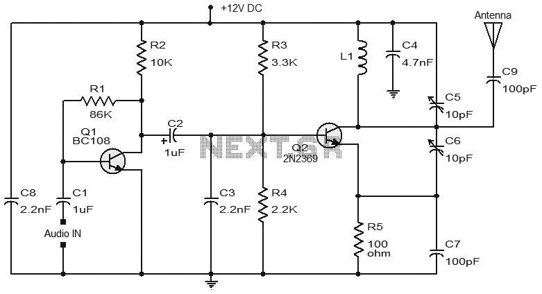
The described FM transmitter circuit is a straightforward design that utilizes two transistors to achieve modulation and amplification of audio signals for FM transmission. The preamplifier stage, utilizing transistor Q1, is critical for amplifying the input audio signal before it is processed further. The collector-to-base configuration allows for stable operation, with R1 and R2 carefully selected to ensure optimal biasing and collector current levels, thereby maximizing the performance of the amplifier.
The coupling capacitor C1 is essential for blocking any DC component of the audio signal, allowing only the AC audio signal to pass through to the base of Q1. This ensures that the transistor operates within its linear region, providing a clean amplification of the audio input.
Following the preamplifier, the oscillator and modulator stage, built around transistor Q2, plays a key role in generating the FM signal. The coupling capacitor C2 connects the amplified audio signal from Q1 to the base of Q2, where it modulates the oscillation frequency. Resistors R3 and R4 are critical for establishing the proper biasing conditions for Q2, ensuring reliable operation in the active region.
The inclusion of the emitter resistor R5 stabilizes the operating point of Q2 and improves linearity, which is crucial for maintaining signal integrity during modulation. The tank circuit, composed of inductor L1 and the trimmer capacitor C5, is vital for generating oscillations at the desired frequency. The trimmer capacitor allows for fine-tuning of the oscillator frequency, enabling the transmitter to operate at a specific FM band frequency.
Finally, the modulated FM signal is made available at the collector of Q2. Capacitor C9 facilitates the coupling of this signal to the antenna, allowing for efficient transmission of the FM signal over the airwaves. Overall, this simple two-transistor FM transmitter circuit exemplifies a fundamental approach to FM transmission, suitable for various applications in amateur radio and educational projects.A lot of FM transmitter circuits have been already published here. This just another one, a simple two transistor FM transmitter. The first stage of the circuit is a preamplifier stage based on transistor Q1. This is a collector to base biased amplifier stage where resistor R2 sets the collector current and R1 provided the necessary collector to ba se bias. C1 is the input DC decoupling capacitor which couples the input audio signal to the Q1 base. C8 is the power supply by-pass capacitor. Next stage is the oscillator cum modulator stage built around transistor Q2. Electrolytic capacitor C2 couples the output of the first stage to the second stage. R3 and R4 are the biasing resistors of Q2. R5 is the emitter resistor of Q2. Inductor L1 and trimmer capacitor C5 forms the tank circuit which is necessary for creating oscillations. The modulated FM signal is available at the collector of Q2 and it is coupled to the antenna using capacitor C9.
🔗 External reference
Related Circuits
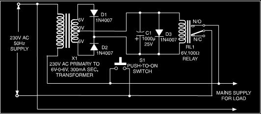
This is a low-cost protection circuit designed to safeguard electrically operated home appliances, such as TVs, DVD players, refrigerators, and other devices, during sudden power outages and the subsequent restoration of mains supply. Appliances like refrigerators and air conditioners...
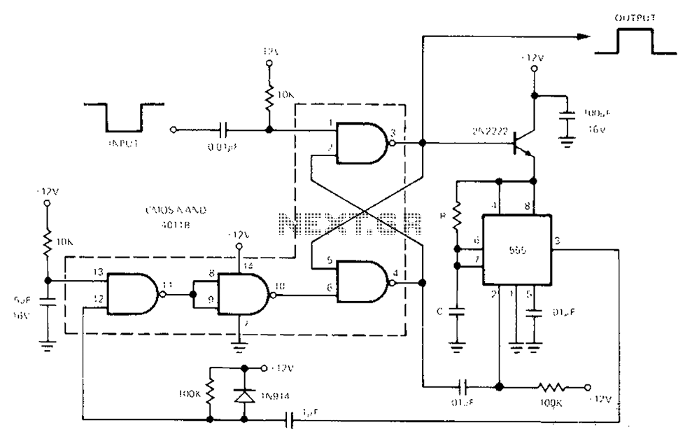
The 555 Timer facilitates a low-loss single-shot circuit and interfaces with the CMOS4011B NAND gate circuit. The standby power consumption is less than 50 µA. When the one-shot circuit is activated, the current consumption is 4.5 mA, and the...

The basic application circuit for a thermistor is illustrated. Figure (a) depicts a fundamental temperature measurement circuit with limited accuracy, suitable only for applications that do not require high precision. RT represents a positive temperature coefficient thermistor; as the...
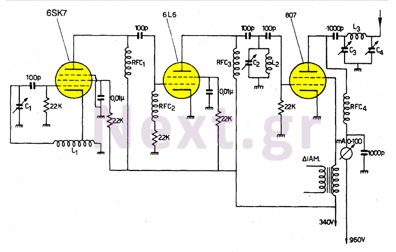
This transmitter operates in the shortwave range from 6 MHz to 22 MHz. Coil L1 serves as the shortwave oscillating coil for the 6SA7 vacuum tube and is commercially available. Capacitor C1 is a variable capacitor with a capacitance...
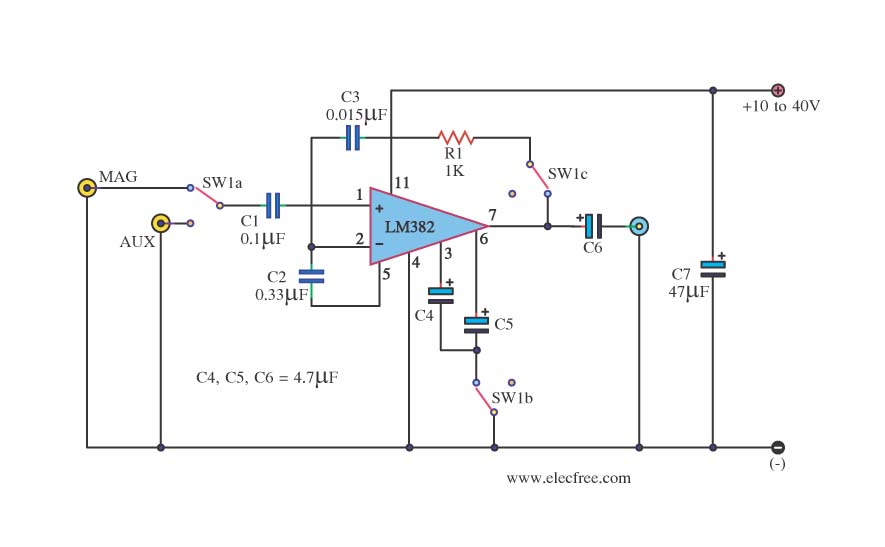
This is a simple preamplifier circuit. It can accept a general AUX sound signal as well as a signal from a microphone. The purpose of the circuit is to amplify the sound signal at the initial stage using an...
The AR-300 DC arc welding machine circuit includes the AX, AX1, AX3, and AR series. The structure of these machines is fundamentally similar, consisting of a three-integral unit converter, a phase asynchronous motor, and a DC arc welding generator...