
phase lock loop frequency synthesizer
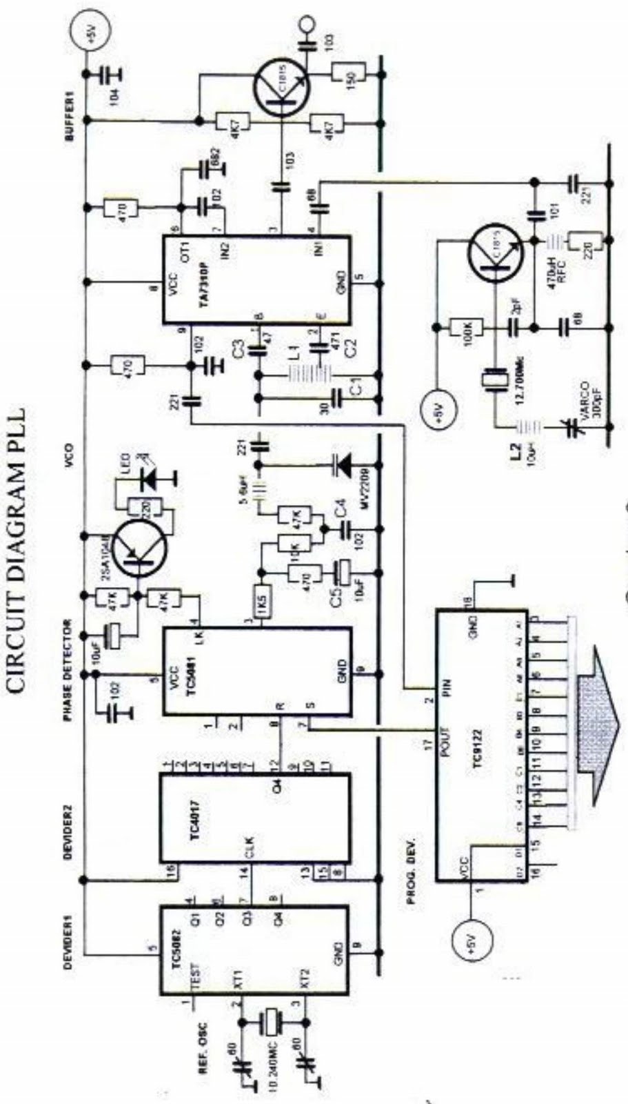
The PLL design described involves a systematic approach to frequency synthesis and phase comparison, ensuring precise control and stability. The phase detector continuously monitors the phase relationship between the reference and VCO signals, generating an error signal proportional to the phase difference. This error signal is filtered by the loop filter, which smooths out rapid voltage changes, thereby providing a stable control voltage to the VCO. The VCO, in turn, generates a frequency that is adjusted based on the control voltage, ensuring that the output frequency aligns with the desired reference frequency.
The loop filter's design is critical, as it determines the transient response and stability of the PLL. A well-designed loop filter can effectively dampen oscillations and provide a stable output, while a poorly designed filter may result in instability and oscillatory behavior. The choice of components, including the varactor diodes and the programmable divider, further influences the PLL's performance, allowing for fine-tuning of the output frequency and ensuring that the system can accommodate variations in input conditions.
In conclusion, the PLL design outlined integrates various components and principles of phase detection, frequency division, and voltage control to achieve accurate frequency synthesis. This design serves as a practical example of how PLLs can be utilized in communication systems, providing essential functionality in frequency modulation and demodulation applications. The careful selection of ICs and the attention to loop filter design contribute significantly to the overall effectiveness and reliability of the PLL circuit.Major role in the PLL phase detector is held by the duty comparing the input phase of the VCO signal with a reference signal and the output is a different phase. The existence of different phases will provide a further voltage difference, the difference voltage is filtered by the loop filter and applied to VCO.
Then the control voltage to the VCOfrequency change towards minimize the difference between a reference signal with a feedback signal from VCO. If the loop becomes locked, then control voltage in a position where the average frequency of feedback signal exactly equal to the frequency reference. The success of a PLL design is largely determined by the loop filter design good. This is because in the event of phase difference, phase detector, voltage differences will issue a change up and down.
Loop filter must be able to hold sway voltage so that voltage changes into the VCO becomes smooth. various PLL can we make, but in this paper try asking a PLL design with a detailed circuit so that we can easily understand how it works. Although to fulfill that purpose is required of Actually PLL circuit can be made with a fairly simple example using IC type MC145106, MC145163, and so forth there are also many on the market.
These type of IC has been able to perform the function is complete, with an IC is able to perform the functions of the TC9122, TC5081, TC5082 and TC4017. But the use of IC type is not discussed in this paper. In this paper proposed a PLL design with step 1 KHz fine equipped with an analog tuner with band width of 1 to 2 KHz to allow setting more precise operating frequency (less than 1 KHz).
PLL is planned to be able to work from 13, 700 to 14, 699 MHz for use in transceiver with carrier oscillator or 10. 7 MHz SSB filter. Working frequency is set with three-digit thumb wheel such that the number of hundreds, tens and units of KHz on the display thumb wheel can immediately show operating frequency transceiver.
If we have described, the PLL consists of several parts is generating reference frequency (1KHz), phase detector, loop filter, VCO, programmable oscillator mixing DEVIDER and feedback. As a reference frequency generator used to charge TC5082 raised frequency of 10 KHz and the duty to share TC4017 frequency 10KHz results from TC5082 to 1KHz.
1KHz frequency is then used as comparison phase by phase detector TC5081. For VCO in this design is used TA7310. The use of IC is intended to be at once doubled as the mixer for the purposes of feedback on the phase detector through a programmable DEVIDER. In this design the input to the programmable DEVIDER a result of the reduction of the frequency VCO with frequency crystal.
Frequency VCO and band width is set according to the needs in this design he should be able to work at a frequency of 13, 700 MHz to 14, 700 MHz, for used on instrument with 10. 7 Mc IF. As a control frequency of the VCO varactor diodes are used. Various types of varactor can be used for example MV2205, MV2209, BA150, SMV 610 and so on. Type varactor diode of the above have a capacitance range different which can be seen in vademicum issued by the manufacturer.
Programmable devider share feedback from the VCO frequency by a factor of divider as we enter the program, the results are fed into the phase detector and compared with the reference signal. As a programmable DEVIDER TC9122 use, type of IC has the ability to share with the divisor factor until 3999.
Therefore, feedback from the VCO can not be directly input to TC9122 and must first be mixed with an oscillator frequency and the result is inputted into devider. Frekuensi mixer oscillator must be chosen so that the reduction does not exceed the ability of TC9122.
For example, the PLL design is planned to work on 13, 700 MHz to 14, 699 MHz oscillator used mixing 12, 700 MHz (the difference is 1-1999 MHz). TC9122 programming done Binary coded Decimal (BCD) is that any decimal numb 🔗 External reference
Related Circuits
The circuit primarily consists of two Butterworth filters, designed to create a feedback amplifier with a gain of approximately 0.707. It features a differential input amplifier, where one input is grounded, resulting in a single input terminal. The attenuation...
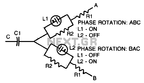
A simple, portable phase-sequence indicator is designed to determine the correct phase rotation in polyphase circuits. The primary components include two neon lamps, two resistors, and a capacitor. During operation, the leg voltages are unbalanced, causing the lamp with...
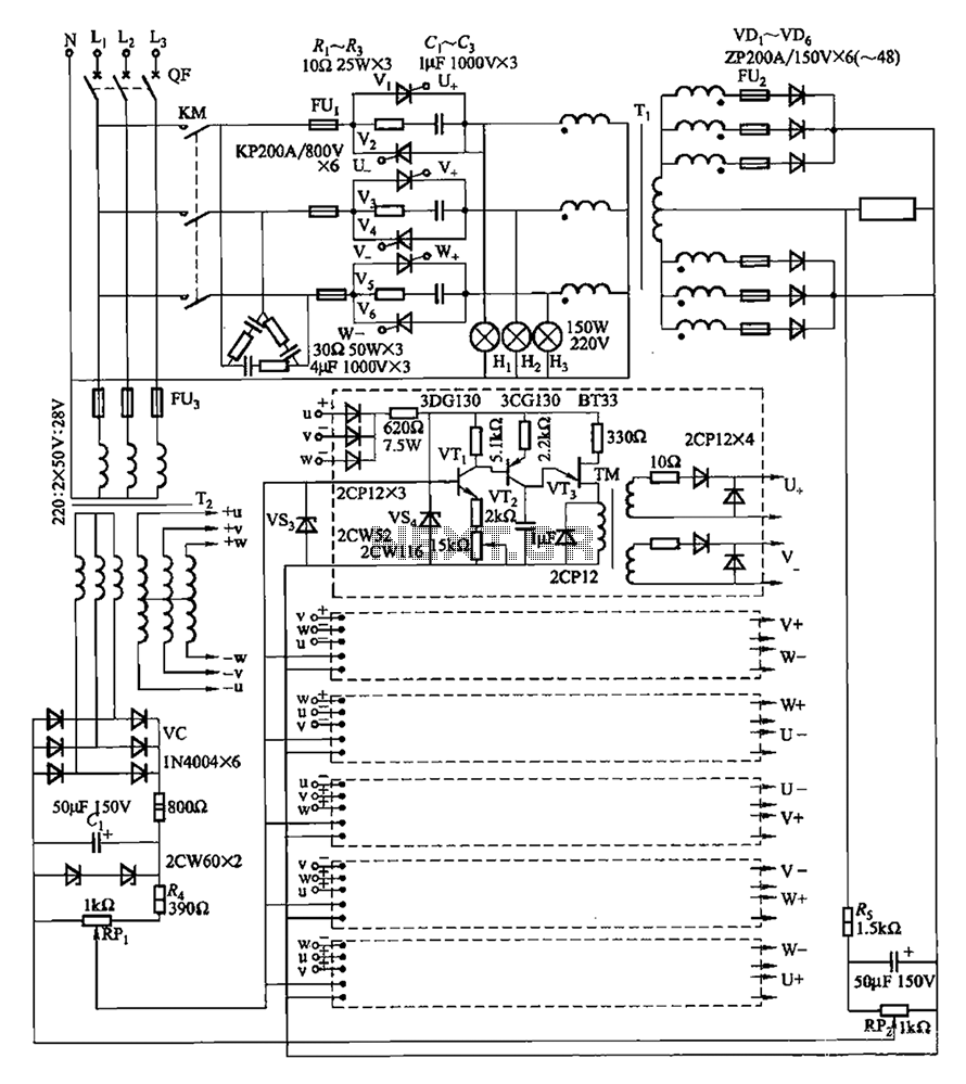
A three-phase thyristor power regulator circuit designed for plating applications, capable of handling currents from 1200A to 6000A at a voltage of 10V. The circuit comprises a main circuit, a trigger circuit, synchronous power components, and a voltage negative...
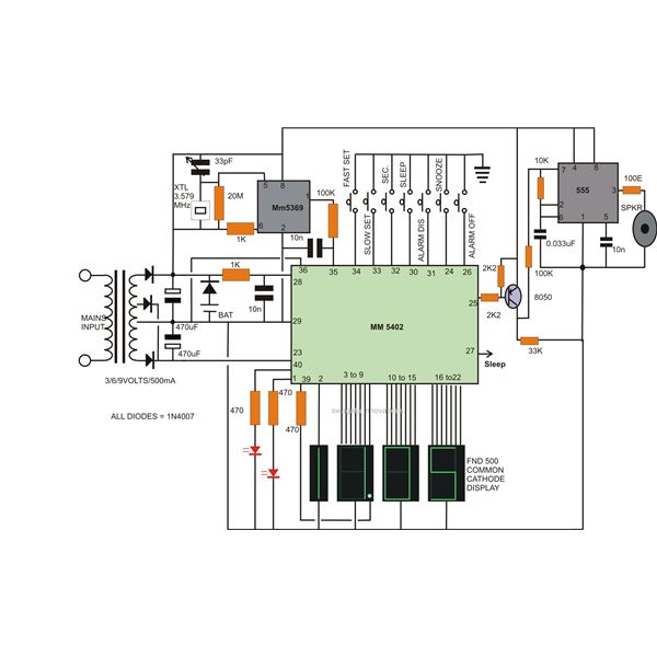
Creating a high-end, precise digital LED clock is now as straightforward as preparing noodles. This article outlines the process of constructing a digital clock using readily available electronic chips, such as the National Semiconductor MM5402 clock IC, along with...
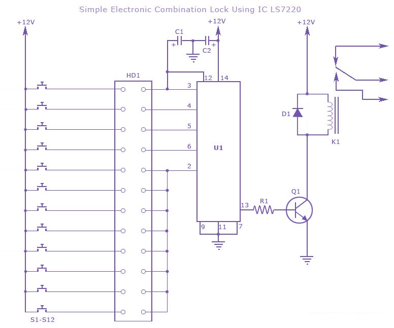
A simple electronic combination lock using the IC LS7220. This circuit employs a relay to control any device when a combination of four digits is entered. Keypads serve as the input method for entering the digits, and the correct...
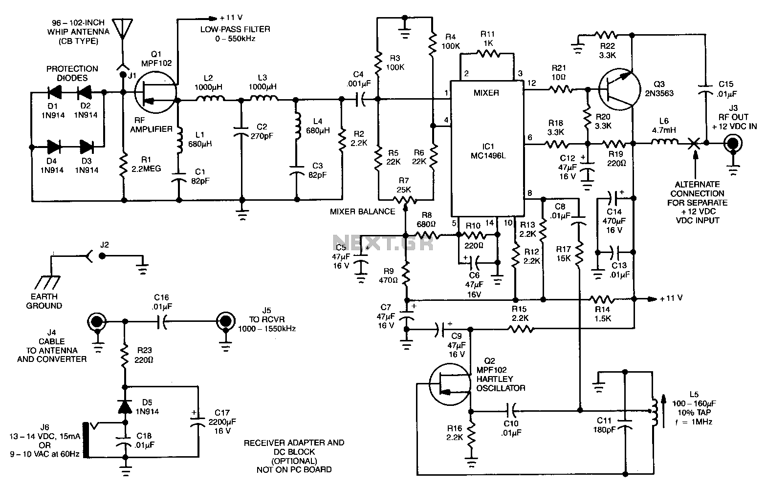
The signals below 550 kHz include maritime mobile, distress signals, radio beacons, aircraft weather information, European Longwave-AM broadcasts, and point-to-point communications. A low-frequency converter transforms the 10 to 500 kHz LW range into a 1010 to 1550 kHz MW...